Memory Industry Reviews HBM Hybrid Bonding ... Applied Expands Equipment Business
IT DAILY ·
✦ AI Summary
Global memory manufacturers are reviewing hybrid bonding for HBM applications.
Applied Materials said memory customers are evaluating hybrid bonding technology for HBM.
Applied can respond to about 80% of the process steps related to hybrid bonding and is jointly developing related technologies with BE Semiconductor Industries.
BizCrushWant to follow Korean talks and live streams in real time?Try CapCrush on the web
As the number of stacking layers in HBM increases and performance requirements rise, the need to improve chip-to-chip interconnect density and boost power efficiency is growing. Against this backdrop, global memory makers are reviewing hybrid bonding for HBM applications. Hybrid bonding is regarded as a next-generation bonding technology.
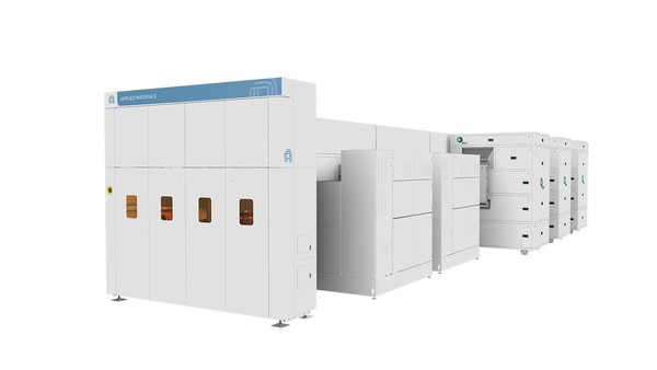
According to the semiconductor industry on the 13th, Applied Materials has begun expanding its related equipment business in line with this trend. The 'Kinex' hybrid bonding system is equipment jointly developed by Applied Materials and BE Semiconductor Industries. The system is an advanced packaging tool for direct chip-to-wafer bonding.
Applied Materials held its fiscal 2026 fourth-quarter earnings conference call on the 12th, local time. During the call, Applied Materials said memory customers are evaluating hybrid bonding technology for HBM.
Bryce Hill, CFO of Applied Materials, said that all of Applied's memory customers are evaluating ways to apply hybrid bonding to HBM. He explained that the timing of mass production adoption of hybrid bonding is a matter for each customer to decide.
Hybrid bonding is a technology that directly bonds the metal connections and insulating layers of semiconductor chips and wafers. Conventional thermo-compression bonding uses protruding metal connection bumps. By contrast, hybrid bonding can eliminate or reduce bumps, making it possible to narrow chip-to-chip connection spacing and shorten wiring lengths. These effects can improve interconnect density and power efficiency.
HBM achieves high data-transfer bandwidth through a structure in which multiple DRAM chips are vertically stacked. As the number of HBM layers increases, the importance of chip-to-chip interconnect density and thermal management also grows. Under such conditions, mass-producing hybrid bonding requires high bonding precision, surface flatness, and contamination control.
Applied is a major global supplier of equipment across semiconductor manufacturing, including deposition, etching, and planarization. Revenue in fiscal 2026 rose 21% from a year earlier to USD 34.446 billion. Revenue in Korea came to USD 6.362 billion, accounting for 18% of total revenue.
With major production facilities of Samsung Electronics and SK hynix in Korea, the country is mentioned as one of Applied's key markets. Applied expects equipment demand to rise as technology shifts unfold.
CEO Gary Dickerson said on the conference call that the company can respond to about 80% of the process steps related to hybrid bonding. This roughly 80% does not refer to market share, but to the range of process steps for which equipment supply is possible. Applied has secured deposition and chemical mechanical polishing (CMP) as technologies needed before and after bonding, and it is jointly developing hybrid bonding and next-generation chip interconnect technology with BE Semiconductor Industries, a Dutch semiconductor assembly equipment maker.
The two companies expanded the scope of their cooperation in October to next-generation interconnect and packaging technologies. Applied announced a stock purchase agreement on October 26 to push ahead with increasing its stake in BE Semiconductor Industries by about 20%. The equity acquisition is expected to proceed in line with related regulatory procedures.
The latest earnings showed higher demand for memory and advanced packaging equipment. Revenue in the semiconductor systems segment for fiscal 2026's fourth quarter was USD 7.996 billion, up about 64% from a year earlier. DRAM-related revenue accounted for 33%, up 5 percentage points from 28% in the same period a year earlier.
The company said it recorded its highest quarterly revenue in the DRAM segment and in the advanced packaging segment during the period. Revenue in the Korea semiconductor systems segment and the Taiwan semiconductor systems segment also reached quarterly highs. However, it did not disclose the share of HBM-related equipment in Korea revenue.
Applied forecast that revenue from its advanced packaging business in calendar 2026 will increase by about 90%. Hill, the CFO, explained that a significant portion of the business's growth comes from HBM-related areas. CEO Dickerson said HBM demand is expected to remain solid in 2027.
The timing for mass production adoption of hybrid bonding for HBM has not been decided, but if memory makers shift their bonding methods, equipment demand could expand across pre- and post-bonding processes such as bonding, deposition, and planarization. Applied's technology collaboration with BE Semiconductor Industries and its equity investment in BE Semiconductor Industries provide a foundation for expanding its business base across the related process chain.
Source: IT DAILY · Kim Byung-ju
Original: https://www.itdaily.kr/news/articleView.html?idxno=242930
References
This article was produced with the help of an automated content generation algorithm.
Source: IT DAILY
View originalThis article was summarized and organized by BizCrush based on the original article from IT DAILY. For exact quotations and full details, please refer to the original article.
Keep reading
BizCrush