T-Robotics CEO Ahn Seung-wook: “Targeting the TGV Glass Substrate Market With OLED Transfer Technology”
TECHWORLD ·
✦ AI Summary
T-Robotics is a developer of vacuum robots and transfer modules for semiconductor and display manufacturing processes, and it is expanding its application scope into glass substrates and PLP based on the vacuum and precision transfer technology it accumulated on large OLED production lines.
The company unveiled a vacuum transfer robot and a contactless atmospheric robot for glass substrates, as well as an EFEM for PLP, while explaining its high-load, high-precision technology for moving large glass substrates.
T-Robotics is conducting combined vacuum-and-atmospheric robot performance evaluations with major domestic semiconductor equipment makers, and it is also seeking entry into the Chinese glass substrate market based on business relationships with BOE, CSOT, Tianma, and more than 700 vacuum robots supplied to China.
T-Robotics is a developer of vacuum robots and transfer modules for semiconductor and display manufacturing processes, and it has vacuum and precision transfer technology accumulated on large OLED production lines. As investment in AI semiconductors and advanced packaging expands, T-Robotics is broadening the application of its existing display equipment technology to glass substrates and PLP.
T-Robotics is expanding the application of that technology to the glass substrate market for next-generation semiconductor packaging. In South Korea, the company is conducting product evaluations with semiconductor equipment makers.
In China, the company has a customer base built in the display market, and it is using that to pursue entry into the local glass substrate equipment market. T-Robotics is moving to target the Chinese market based on its existing customer base.
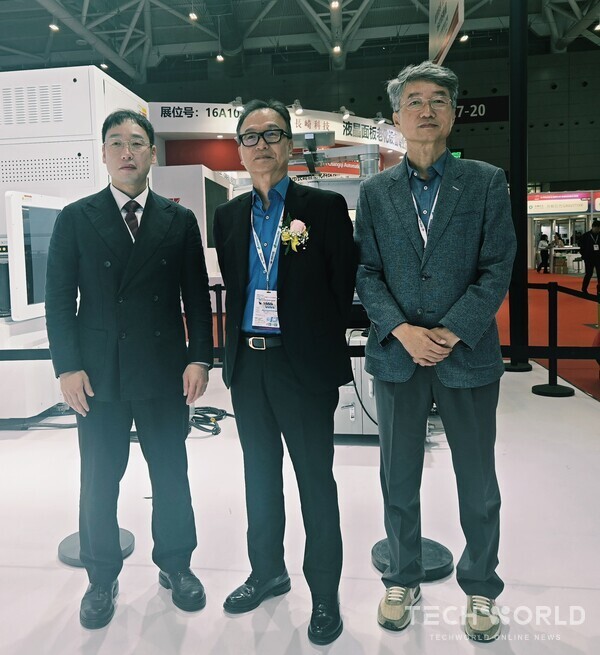
T-Robotics CEO Ahn Seung-wook spoke on Oct. 27 at the company's booth at the C-Touch & Display Shenzhen 2026 event in Shenzhen, China. At the event, he explained the current status of robot development for TGV glass substrates and the company's future business strategy.
At the exhibition, the company showcased a vacuum transfer robot and a contactless atmospheric robot for glass substrates, presenting its vacuum and contactless robot technologies for glass-substrate handling. The items on display also included an EFEM for PLP aimed at large glass substrates.
The EFEM for PLP applies vacuum on the underside of the substrate and a contactless method on the top. The dedicated vacuum robot for glass-substrate transfer has a six-axis structure and can handle a 20 kg load, including the fork. Its X, Y, and Z-axis repeatability is at the ±0.3 mm level, and it uses a parallel-link-based structure. This parallel-link-based structure enables multidirectional substrate transfer in a vacuum environment.
Glass substrates become more difficult to manage in terms of load, sagging, and vibration as they become larger and heavier than conventional semiconductor wafers. Ahn said that while conventional semiconductor wafers are extremely light, large glass substrates weigh more than 10 kg, making robot technology capable of withstanding heavy loads necessary.
T-Robotics is simultaneously developing a transfer robot for inside vacuum chambers and a contactless robot for atmospheric sections. The atmospheric transfer method lifts the glass substrate by about 0.2 mm using air, with the goal of reducing direct contact between the substrate and the robot hand.
The company regards the vacuum transfer experience it accumulated on large OLED production lines as its core foundation. Its technology base is the transfer experience from large OLED production lines, and T-Robotics has supplied vacuum transfer robots for display processes from Generation 4 to Generation 10.5 and above.
In particular, it has accumulated handling technology for large plates and masks in a high-vacuum environment in Generation 8.6 OLED processes. The vacuum transfer robot for Generation 8.6 OLED can handle a maximum load of 240 kg excluding the fork, operate in environments up to 500 C, and has a five-axis structure. Its X, Y, and Z-axis repeatability is also ±0.5 mm. Ahn said the company accumulated heavy-load precision control technology through handling 200 kg-class masks and plates in Generation 8.6 OLED processes.
That experience in heavy-load, high-temperature, vacuum-environment transfer is being applied to glass substrate equipment development. Ahn explained that, based on that experience, the company is developing vacuum and contactless transfer technologies for glass-substrate processes.
T-Robotics is pursuing a strategy of supplying vacuum robots and contactless atmospheric robots at the same time. The vacuum robot is responsible for transferring substrates inside the vacuum chamber, while the contactless atmospheric robot handles substrates outside the chamber. The company is also envisioning a system that links transfer equipment for atmospheric sections and vacuum sections, with glass-substrate processes as the target application.
Ahn said the company can supply both a vacuum robot for inside-vacuum-chamber transfer and a contactless atmospheric robot linked with an external load lock chamber. It was reported that T-Robotics plans to broaden the scope of its response by bundling and supplying robots needed for both vacuum and atmospheric sections.
T-Robotics has completed patent registration for its related robot structure in South Korea, the United States, China, and Japan. The technology development phase has entered the customer evaluation stage.
T-Robotics is currently conducting performance evaluations with major domestic semiconductor equipment makers. The evaluation method involves a combined vacuum-and-atmospheric robot configuration. Ahn said that, although details are confidential, the company is conducting combined vacuum-and-atmospheric robot evaluations with major domestic semiconductor equipment makers.
Alongside its domestic evaluations, T-Robotics is pursuing entry into the Chinese market. Through its display equipment business, the company built business relationships with Chinese panel makers such as BOE, CSOT, and Tianma, and it has supplied more than 700 vacuum robots to China. The company plans to connect its existing customer network and local business experience to the glass substrate sector. Ahn said the company is pursuing cooperation with Chinese glass substrate customers based on its business relationships with major Chinese display panel makers such as BOE, CSOT, and Tianma.
In China, investment in Generation 8.6 IT OLED is under way. Investment in equipment related to advanced packaging based on glass substrates is also under way there. Against this backdrop, T-Robotics aims to expand into the glass substrate business as well, leveraging customer relationships and supply achievements secured in its Chinese display equipment business.
At this exhibition, equipment related to glass-substrate processing, deposition, lamination, inspection, and transfer was presented at the same time. Glass-substrate technology has advanced to the pilot-line and customer evaluation stages. Accordingly, the areas in which transfer equipment makers can participate are also expanding.
Based on the technology and factory automation experience it has accumulated in the display equipment sector, T-Robotics is broadening its application areas to semiconductor packaging and logistics automation, while moving to expand into new businesses with glass substrates and autonomous mobile robots (AMR). The company has set its expansion areas as semiconductor packaging and logistics automation, based on the precision control technology of its display vacuum robots and its factory automation experience, and it plans to diversify its business structure through this effort.
The next step in the glass substrate business is to turn the ongoing customer evaluations into actual supply contracts. In this process, the company sees value in validation with domestic equipment makers and in using the customer network it has built in the Chinese display market, and it expects to expand its business scope from existing display equipment to semiconductor advanced packaging equipment accordingly.
Source: TECHWORLD · Kim Seung-gi
Original: https://www.epnc.co.kr/news/articleView.html?idxno=409142
References
This article was produced with the help of an automated content generation algorithm.
Source: TECHWORLD
View originalThis article was summarized and organized by BizCrush based on the original article from TECHWORLD. For exact quotations and full details, please refer to the original article.