Lee Jae-yong Inspects Next-Generation Semiconductor Packaging in Japan, Boosts AI Tech Competitiveness
TECHWORLD ·
✦ AI Summary
Samsung Electronics Chairman Lee Jae-yong visited Advanced Package Lab(APL) in Yokohama, Japan, on the 1st to review the progress of next-generation semiconductor packaging technology development.
Lee reviewed the status of development of advanced package materials and process element technologies with APL researchers and discussed cooperation with Japan's materials, parts and equipment industry.
Samsung Electronics plans to develop APL into a global R&D base for next-generation packaging element technology development and to pursue the development of next-generation process and materials technologies such as wafer bonding and glass substrates.
Samsung Electronics Chairman Lee Jae-yong visited Japan. The purpose of the visit was to review the progress of next-generation semiconductor packaging technology development and to explore ways to strengthen cooperation with Japan's materials, parts and equipment industry.
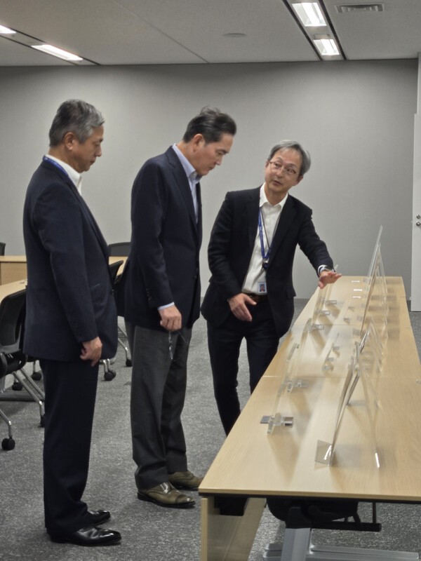
According to Samsung Electronics, Chairman Lee visited 'Advanced Package Lab(APL)' in Yokohama, Japan, on the 1st. APL is Samsung Electronics' cutting-edge semiconductor packaging research base in Yokohama and its packaging research base in Japan. At the lab, Lee reviewed the status of research into next-generation packaging element technologies.
Lee checked the status of development of advanced package materials and process element technologies with APL researchers. He also discussed cooperation with Japan's materials, parts and equipment industry. Lee stressed the importance of securing related technologies and urged continued technology development, saying that in the AI era, advanced packaging technology is emerging as a core factor in semiconductor competitiveness.
APL officially opened on September 8. This visit came about two months after the opening, and it carries significance as Lee's first on-site inspection since APL opened.
Samsung Electronics established APL in Yokohama in 2023. The purpose of APL's establishment is research into package element technologies. Samsung Electronics is investing a total of JPY 40 billion(about KRW 350 billion) over 5 years from 2024, and the investment is aimed at building an R&D base in Japan.
APL is an organization that develops and verifies core element technologies such as materials and processes for advanced semiconductor packaging. APL serves as an R&D base and also connects Samsung Electronics' semiconductor design and manufacturing capabilities with Japan's materials, parts and equipment technology ecosystem.
Samsung Electronics plans to expand APL's research areas. The areas it plans to pursue include developing next-generation process and materials technologies such as wafer bonding and glass substrates, as well as developing a new high-performance packaging architecture for mass production of low-power, high-performance semiconductors in the AI era. Samsung Electronics is also considering expanding APL's role.
Samsung Electronics plans to differentiate the research areas from its package research organization under the semiconductor research institute in South Korea. At the same time, it is envisioning close cooperation between the two organizations. The goal of the collaboration is to create R&D synergies.
Samsung Electronics is building a cutting-edge packaging research base in Japan and continuing to invest there. The company plans to steadily expand its local research workforce. In addition, Samsung Electronics plans to develop the Yokohama APL into a global R&D base for next-generation packaging element technology development.
The background to this move is Japan's semiconductor industry ecosystem. Japan is home to many companies with world-class technological capabilities in the semiconductor materials, parts and equipment sectors. Japan has also established a foundation for industry-academia-research collaboration.
The Japanese government has also designated the semiconductor and AI industries as strategic sectors. It is also pursuing investment and support policies. The competitiveness of the local semiconductor ecosystem is cited as a reason Samsung Electronics is maintaining its research base in Japan and continuing to invest there.
Yokohama is a large city adjacent to Tokyo. It is home to many excellent universities and research institutions, making it advantageous for securing specialized researchers. It also has a concentration of materials and equipment companies related to advanced packaging, making it an appropriate region for promoting technical cooperation with related companies.
Samsung Electronics plans to leverage Yokohama's excellent talent pool and industry-academia-research infrastructure. Based on that, Samsung Electronics plans to develop APL into a research collaboration hub that connects Japanese materials and equipment companies with Samsung Electronics' semiconductor technology capabilities.
As demand for AI computing surges, competition to improve semiconductor performance is expanding beyond advanced process nodes into packaging technology. Accordingly, the importance of efficiently connecting and integrating multiple chips is also growing. Advanced packaging is emerging as a core technology that determines the performance and efficiency of AI semiconductors.
In particular, as changes in bandwidth, power efficiency and heat dissipation characteristics have been observed in the process of integrating heterogeneous semiconductors such as GPU, HBM and AI accelerators into a single package, the importance of advanced packaging is increasing. These changes in the integration process of heterogeneous semiconductors are further raising the importance of packaging technology.
In line with this trend, Samsung Electronics is pushing ahead with securing core technologies for materials and equipment for advanced packaging based on its memory and logic semiconductor technologies. Samsung Electronics' strategy is aimed at strengthening the competitiveness of next-generation products.
Source: TECHWORLD · Park Kyu-chan
Original: https://www.epnc.co.kr/news/articleView.html?idxno=409053
References
This article was produced with the help of an automated content generation algorithm.
Source: TECHWORLD
View originalThis article was summarized and organized by BizCrush based on the original article from TECHWORLD. For exact quotations and full details, please refer to the original article.