Common Ground for Cars and Robots’ AI: Bigger Substrates, Finer Circuits
IT DAILY ·
✦ AI Summary
As the scope of AI expands to cars and robots, the specifications of semiconductor substrates and sensing components are also changing.
Daeduck Electronics unveiled roadmaps for FC-BGA for physical AI and FCCSP for automotive radar at KES 2026.
LG Innotek exhibited a prototype fusion sensing module that integrates an RGB camera and IR sensing into a single module.
As the scope of AI expands to real-world machines such as cars and robots, the specifications of the electronic components that make them up are also changing. AI-powered automotive and robot operation requires semiconductors that can rapidly process information from surrounding-awareness sensors and input data, and this is leading to changes in high-performance semiconductor substrates that require more stable transmission of signals and power.
These changes were also visible at the component level at the Korea Electronics Show (KES 2026) held on the 14th at COEX in Seoul. Daeduck Electronics unveiled its next-generation technology roadmap for semiconductor package substrates for autonomous vehicles and humanoid robots, while LG Innotek unveiled an automotive module that integrates and miniaturizes multiple sensing functions.
Daeduck Electronics said the common structure of autonomous vehicles and humanoid robots consists of sensor-based surrounding awareness, information processing by AI semiconductors, and actuation by the drive system. Against the backdrop of this structural commonality between autonomous vehicles and humanoid robots, component technologies first applied to cars are spreading to robots, and the points of contact between component technologies for different devices are also expanding.
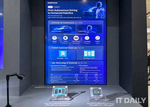
Daeduck Electronics unveiled its roadmap for FC-BGA and related technologies for physical AI at KES 2026. The photo credit reads: Reporter Kim Byeong-ju.
Along with the exhibition, Daeduck Electronics presented future specification changes for FC-BGA for physical AI. FC-BGA is a package substrate that connects high-performance semiconductors such as CPU and ASIC to the main board.
As a development direction for FC-BGA for physical AI, Daeduck Electronics presented larger sizes and more layers to match improvements in AI semiconductor performance. That is because as the computational performance of AI semiconductors rises, the amount of signal transmission and power delivery required by the substrate increases. Expanding the substrate area and using a multilayer circuit structure are intended to address these increased signal and power demands.
According to Daeduck Electronics' roadmap, this year's FC-BGA will be up to 65×65 mm with 22 layers. In 2027, FC-BGA will expand to 75×75 mm with 26 layers. In 2028, FC-BGA was presented at 85×85 mm with 30 layers.
The bump pitch connecting semiconductors and substrates is currently about 140 μm. The bump pitch roadmap was presented at about 130 μm in 2027 and about 110 μm in 2028. As the computational performance of AI semiconductors rises, substrates are becoming larger, layer counts are increasing, and bump pitch is becoming tighter.
As a solution for large-area, high-layer-count substrates, it was pointed out that size and layer expansion alone are not enough. The challenges for large-area, high-layer-count substrates were identified as suppressing warpage, ensuring stable signal and power transmission, and managing heat.
Daeduck Electronics presented the main technical challenges for FC-BGA as high-speed input/output, memory bandwidth, power integrity, and warpage and thermal control for large-area packages. This was explained in the context that simply increasing substrate size and layer count alone is difficult to address.
Other changes were also seen in flip chip chip scale package (FCCSP) for automotive radar. The direction of FCCSP for automotive radar has been set toward finer circuits within a limited space rather than larger substrates.
According to the roadmap unveiled by Daeduck Electronics, the line width/spacing of fine circuits in mass-produced products this year is 8/10 μm. The line width/spacing of fine circuits in next-generation products is 6/8 μm. The target line width/spacing of fine circuits in 2027 is 5/5 μm, and the target line width/spacing of fine circuits in 2028 is 4/5 μm.
The pad and via size is currently 60/80 μm, with a 2028 target of 40/62 μm. The solder-on-pad (SOP) pitch is currently 55 μm, with a target of 35 μm in 2028.
FCCSP is a package substrate for flip-chip connection between semiconductor chips and substrates. Daeduck Electronics presented fine line width/spacing, microvias, and high reliability as the core technologies for automotive FCCSP.
Daeduck Electronics also presented a roadmap for future application areas. The direction runs from advanced driver assistance systems (ADAS) and automotive radar to millimeter-wave sensors and humanoid sensors.
This is linked to a plan to apply high-frequency, high-reliability substrate technology for automotive surrounding awareness to the robot sensing sector. It is a trend that broadens the scope of technologies used in vehicle sensors.
At the exhibition site, LG Innotek unveiled its future mobility exhibit area for KES 2026. At the LG Innotek booth, changes in sensing components mounted directly in vehicles could be seen. The photo credit reads: Reporter Kim Byeong-ju.
In the semiconductor substrate sector, technology development is under way to accommodate more circuits. In the sensing components sector, there is a trend toward reducing space by integrating multiple functions into a single module. A direction was also presented to integrate separate camera and IR configurations into one module.
LG Innotek exhibited a prototype fusion sensing module for driver status detection. Previously, the configuration had a separate RGB camera and infrared (IR) sensing, but this product integrates RGB camera and IR sensing into a single module. Through this, it was designed to detect the driver's face and condition by using RGB images and IR sensing at the same time.
LG Innotek reduced the size of the new module by integrating multiple sensing functions. This also reduces the space occupied by vehicle interior components. An LG Innotek official said the new module's size has been cut by nearly half compared with the previous exhibition product.
LG Innotek is pushing to secure sensing data for verification in real-road environments. The equipment mounted on its data-collection vehicles includes cameras, radar, and lidar, and the company is collecting road-, object-, and weather-related data while driving in the capital region. It plans to expand the number of data-collection vehicles to about 20 by 2028.
The fusion sensing module placed at the exhibition remains at the prototype stage, so the actual vehicle models that will use the module and the mass-production schedule have not yet been decided. LG Innotek plans to introduce a composite sensing solution that combines automotive cameras, radar, and lidar into the physical AI sector.
Source: IT DAILY · Kim Byeong-ju
Original: https://www.itdaily.kr/news/articleView.html?idxno=242190
References
This article was produced with the help of an automated content generation algorithm.
Source: IT DAILY
View originalThis article was summarized and organized by BizCrush based on the original article from IT DAILY. For exact quotations and full details, please refer to the original article.