SK Hynix to Move Beyond HBM With HBF and 3D-Stacked DRAM, Reshaping the AI Memory Market
TECHWORLD · · 4 views
✦ AI Summary
SK Hynix is broadening its HBM-centered technology competition to HBF, 3D-stacked DRAM and CXL in response to the memory bottlenecks accompanying growth in the AI inference market.
At SEDEX 2026, SK Hynix development chief Ahn Hyun said rising workload complexity, context length and inference request volume will drive stronger demand for AI infrastructure, and predicted that the scale of performance will expand by about 20 times by 2030.
SK Hynix is advancing HBM performance while also pursuing the development of 3D Stacked DRAM, HBF and Storage-Next, along with preemptive HBF standardization and cooperation with global partners.
SK Hynix is expanding its push into the AI memory market beyond HBM to include HBF and 3D-stacked DRAM. To address the memory bottlenecks created by growth in the AI inference market, SK Hynix is broadening the scope of its HBM-centered technology competition and positioning 3D-stacked DRAM, high-bandwidth flash (HBF) and CXL as key next-generation memory technologies. The goal is to expand its reach in the AI memory market.
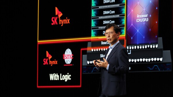
On the 14th, Ahn Hyun, SK Hynix's development chief and president (CDO), delivered the keynote speech at "SEDEX 2026" under the theme "The Direction of Evolution in Memory Technology in the AI Era." Ahn diagnosed the memory bottlenecks that come with growth in the AI inference market and presented a roadmap for next-generation memory technologies. He said that SK Hynix needs to continue strengthening its HBM technological competitiveness amid rising demand for AI infrastructure and also needs to build a new memory layer.
SK Hynix is widening its technology expansion into HBM, 3D Stacked DRAM, HBF, CXL and Storage-Next. Through this, it aims to create a new layer that encompasses multiple memory technologies and improve the performance and energy efficiency of AI infrastructure.
As AI inference demand expands and bottlenecks in data movement between memory layers grow more severe, Ahn identified three factors behind growth in the AI inference market: workload complexity, context length and inference request volume. He said these three factors are increasing together, driving rapid growth in the AI inference market and the infrastructure demand needed to support it.
Ahn said AI infrastructure demand is surging as these three factors combine, and projected that the scale of AI infrastructure performance will expand by about 20 times by 2030.
Ahn said the efficiency gains from AI technology are not limited to cost reduction. He explained that AI efficiency improvements broaden the scope of AI use, create new demand and are a factor driving continued expansion of related infrastructure investment.
Ahn cited the KV cache (Key-Value Cache) as an example of rising memory demand during AI inference. He explained that the KV cache stores and reuses previously processed token information, and that the required memory capacity grows as context length increases.
To improve the efficiency of processing large-scale KV cache data, it is necessary to distribute data across multiple memory layers such as HBM, DRAM and SSD. However, increased data movement between memory layers can hurt performance.
If data movement between memory layers increases, power consumption can also rise. Large-scale KV caches must be split across several memory layers, but the resulting increase in movement creates burdens in both performance and power.
Ahn said bottlenecks are changing in this environment. In the past, the main source of the "Memory Wall" bottleneck was between processors and memory, but in the AI era, he said, the new bottlenecks are the performance gaps between heterogeneous memory layers and the data movement itself.
In response, SK Hynix is pursuing a strategy that goes beyond simply expanding the bandwidth and capacity of individual memory products. It is pursuing technologies that organically connect memory layers and improve data access efficiency.
SK Hynix is also advancing HBM performance. In addition, it has begun developing next-generation technologies to fill the gaps between memory layers, and it has proposed 3D-stacked DRAM and HBF as directions for building the next memory layer.
HBM has continued to evolve from HBM1 to HBM4E, through which it has increased capacity, improved bandwidth and enhanced energy efficiency. At the same time, a major development direction is expanding into Custom HBM for optimizing AI systems for each customer.
Custom HBM is a method that equips the base die with a memory controller and customer-tailored logic. This gives memory a role that goes beyond a simple data storage device, and it is evolving toward function and performance optimization tailored to customer AI architectures.
At the same time, 3D Stacked DRAM was presented as a technology to eliminate the performance bottleneck between SRAM-HBM. 3D Stacked DRAM stacks DRAM on top of logic semiconductors such as GPU and NPU, reducing the physical distance between processors and data. Its key purpose is to supply data for AI model inference from locations adjacent to the processor. As a result, performance gains and lower energy consumption are expected.
HBF is being discussed as a candidate for forming a new memory layer between HBM and DRAM, and it is one of SK Hynix's next-generation memory technologies. The underlying technologies for HBF are TSV stacking technology and high-speed I/O technology accumulated during HBM development. SK Hynix is developing these TSV stacking and high-speed I/O technologies for application to NAND flash.
The development target is about half the bandwidth of same-generation HBM and about 10 times the capacity of same-generation HBM. SK Hynix's strategy is to store larger amounts of data than HBM adjacent to the processor, thereby reducing access to DRAM and SSD. The intended effects are improved overall system performance and better energy efficiency.
AI inference often repeatedly reads large amounts of data, while writes are relatively infrequent. SK Hynix said NAND-based HBF is well suited to the data processing characteristics of AI inference. The company plans to efficiently handle large volumes of data for AI inference and optimize performance and capacity across the memory hierarchy with next-generation memory technologies such as HBF, while also pursuing CXL development and Storage-Next development to build a memory architecture capable of supporting diverse AI workloads.
As conditions for securing a lead in the next-generation memory market, product development and the establishment of an industry ecosystem were cited as important. In next-generation memory competition, product development alone is not enough, so ecosystem building, standardization and cooperation are being pursued together.
In this regard, SK Hynix plans to promote the preemptive standardization of HBF. It also plans to strengthen cooperation with global partners.
As memory technology becomes more diverse, the importance of each layer's performance and capacity, the way layers are connected and the efficiency of the system as a whole is also rising. Accordingly, not only the specifications of individual layers but also the connections between layers and system efficiency are becoming more important.
Ahn said the direction of development in memory competitiveness in the AI era goes beyond improving the performance and capacity of individual products and instead calls for the organic connection of diverse memory layers and maximizing overall system efficiency. This was stated in the context of the growing diversity of memory technologies.
SK Hynix plans to extend the technological competitiveness it has accumulated with HBM to new memory layers. It also plans to support the continued growth of the AI ecosystem through cooperation with global partners.
SK Hynix also unveiled memory solutions for servers, PCs and mobile devices. These plans and disclosures were presented in line with the trend of responding to the next-generation memory market.
SK Hynix participated in SEDEX 2026, hosted by the Korea Semiconductor Industry Association, and showcased memory solutions spanning AI infrastructure as well as PC and mobile customer devices. At the exhibition, SK Hynix adopted "The AI Journey That Never Stops" as its theme.
SK Hynix set up the largest booth at the venue and arranged the exhibition space in the shape of a track. Through this, it designed the visitor flow so that attendees would encounter the brand message, technological vision, global network and major products in sequence.
As server DRAM, it unveiled the "256GB 3DS RDIMM," which addresses AI workloads and delivers the industry's largest capacity. It also showcased the "128GB MRDIMM," which provides high bandwidth, and the "64GB RDIMM," the first in the world to apply a 1c process, a sixth-generation 10-nanometer-class process.
As enterprise SSDs (eSSDs), it exhibited the "PEB210 E1.S 9.5mm" and "PEB210 M.2 2280," both of which support DLC. It also displayed the "PS1101 E3.S 7.5mm," SK Hynix's first QLC-based product.
At the exhibition, it introduced DDR5 CSODIMM, GDDR7, LPDDR5X and LPDDR6 DRAM for PCs and mobile devices, and showcased PC SSDs including PCB01 M.2 2280, PVF01 M.2 2242 and PQF02 M.2 2230. As mobile NAND solutions, it unveiled UFS 4.1 and UFS 5.0. It also prepared exhibits showing the HBM and HBF structures and the history of HBM development, linking its product lineup with its technology roadmap.
The exhibition also featured an NVIDIA Vera Rubin Superchip and an HBM wafer engraved with NVIDIA CEO Jensen Huang's signature. Through this, the company highlighted the partnership between the two companies.
It also introduced social value creation activities using AI technology in local communities and operated an interactive space to experience the future of changes in AI memory technology. Through this exhibition, SK Hynix presented its current competitiveness in AI memory products and also its direction for future next-generation memory technology development.
SK Hynix presented a strategy to expand beyond HBM-centered high-performance memory competition by securing new memory layers such as HBF and 3D-stacked DRAM and optimizing the overall memory architecture. Through this, it set out to respond to infrastructure demand in the AI inference era.
Source: TECHWORLD · Park Kyu-chan
Original: https://www.epnc.co.kr/news/articleView.html?idxno=408181
References
This article was produced with the help of an automated content generation algorithm.
Source: TECHWORLD
View originalThis article was summarized and organized by BizCrush based on the original article from TECHWORLD. For exact quotations and full details, please refer to the original article.