Samsung, SK Hynix Accelerate AI Chip Innovation at Applied’s USD 5 Billion EPIC
TECHWORLD ·
✦ AI Summary
Samsung Electronics and SK hynix will pursue semiconductor technology innovation for the AI era based on Applied Materials’ EPIC Center.
Samsung Electronics plans to engage in technology collaboration across memory, advanced logic, and advanced packaging, while SK hynix plans to accelerate the development of next-generation technologies across DRAM and NAND, including HBM.
The EPIC Center is a collaborative semiconductor process technology and manufacturing equipment R&D facility that will receive a total of USD 5 billion in investment, with Samsung Electronics, SK hynix, TSMC, Intel, and Micron among the founding partners.
Samsung Electronics and SK hynix will pursue semiconductor technology innovation for the AI era based on Applied Materials’ EPIC Center. Samsung Electronics plans to engage in technology collaboration across memory, advanced logic, and advanced packaging. SK hynix plans to accelerate the development of next-generation technologies across DRAM and NAND, including HBM.
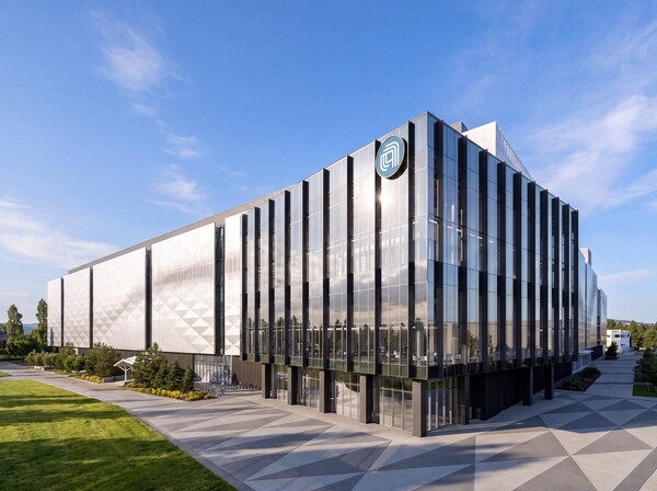
Applied Materials unveiled the EPIC Center on the 12th at its Sunnyvale campus in California and announced the unveiling on the 13th. The EPIC Center is a collaborative semiconductor process technology and manufacturing equipment R&D facility that will receive a total of USD 5 billion in investment. The EPIC Center, the largest of its kind in the world, will be established as a collaborative space where major chipmakers, equipment and systems companies, and university researchers work together.
Founding partners include major chipmakers such as Samsung Electronics, SK hynix, TSMC, Intel, and Micron. Global equipment makers, systems companies, and university researchers will also join. Together with scientists and engineers from Applied Materials, they will jointly develop next-generation semiconductor technologies.
Gary Dickerson, chairman and CEO of Applied Materials, said that the expansion of AI infrastructure and rising demand for high-performance computing are creating unprecedented complexity across semiconductor manufacturing technology development roadmaps. He said the industry needs to rethink and redesign the way it collaborates on the development and commercialization of next-generation semiconductor technologies to win the race for AI leadership.
As a solution, Dickerson said that at EPIC, leading chipmakers, system design companies, equipment partners, and researchers from around the world will work closely with the Applied team. Through this, he said, the goal is to shorten the time from materials innovation to mass production more than ever before.
Samsung Electronics has technology capabilities spanning memory, advanced logic, and advanced packaging. Based on these capabilities, the company plans to accelerate the development and commercialization of next-generation semiconductor technologies at the EPIC Center.
This is because AI chips need higher performance and better power efficiency. To improve AI chip competitiveness, it is important not only to enhance the performance of individual chips, but also to advance memory, compute devices, and chip-to-chip interconnect technologies together.
Sung Jae-hyuk, CTO of Samsung Electronics' DS division, said Samsung is driving the development of computing technologies for the AI era based on its capabilities across memory, advanced logic, and advanced packaging. He said Applied Materials has differentiated process equipment technology and broad expertise across all three areas of memory, advanced logic, and advanced packaging.
Sung outlined a direction in which the two companies, through EPIC, will accelerate the entire process of developing, advancing, and applying innovative technologies in line with the pace of AI technology development. This is aligned with the trend of expanding the existing equipment technology collaboration between Samsung Electronics and Applied at the EPIC Center.
Applied had previously announced that Samsung Electronics would join as a founding partner of the EPIC Center. At that time, Applied presented advanced node scaling, next-generation memory architectures, and materials engineering innovation for ultra-high 3D integration as joint development tasks.
As miniaturization in next-generation semiconductors advances, the importance of not only the devices themselves but also material properties, interfaces, wiring, and process integration is growing. Accordingly, the need for a research and development framework that can address materials research, equipment development, and process optimization together is also expanding.
Against this backdrop, the EPIC Center was designed to carry out materials research, equipment development, and process optimization in parallel. It is expected to serve as a foundation for improving collaboration efficiency in Samsung Electronics' development of next-generation memory, logic, and packaging technologies.
SK hynix plans to use EPIC Center to accelerate innovation in memory technology for the AI era. As AI models grow larger and data processing volumes increase, the importance of memory bandwidth, speed, and capacity for quickly supplying data to processors is rising. To improve the performance of next-generation memory, including HBM, the importance of materials, process, and packaging technologies is also increasing.
Kwak Noh-jung, CEO of SK hynix, said the central challenge of AI computing is delivering data to high-performance processors quickly enough. To that end, he explained, memory with much higher bandwidth, speed, and capacity is needed. SK hynix is pursuing next-generation technology development for HBM, DRAM, and NAND.
SK hynix and Applied are pursuing joint research based on a long-term partnership for next-generation memory technology development. The two companies are expanding their collaborative joint research into materials innovation, process integration, and advanced packaging. Key tasks include improving the performance of next-generation DRAM and HBM, improving the manufacturability of next-generation DRAM and HBM, developing new materials, developing complex integration structures, and developing advanced packaging technologies at the HBM level.
The two companies plan to use the EPIC Center's joint innovation model. Through this, SK hynix engineers and Applied technical staff will work closely together, and the technology development cycle will be shortened. They also plan to link Applied's advanced packaging R&D capabilities in Singapore to connect device-level innovation with heterogeneous integration technologies.
According to the gist of the remarks made at EPIC, this collaboration is meaningful in combining SK hynix's leadership in advanced memory with Applied's leadership in materials engineering and semiconductor manufacturing technology. The two companies plan to respond to key turning points in technology across HBM, DRAM, and NAND, and accelerate memory innovation in the AI era.
The focus of this collaboration is improving memory device performance. However, the partnership will not stop at improving the performance of individual memory products; it will also expand to jointly address technology challenges across AI memory manufacturing, including 3D integration, thermal management, and packaging. The goal is to verify technologies developed in the research phase under conditions similar to actual manufacturing environments and accelerate the transition of next-generation memory to mass production.
To that end, the EPIC Center was designed to carry out the development and commercialization of next-generation semiconductor technologies in a single environment. Under the existing approach, basic materials research, equipment and process development, process integration, and pilot production were conducted in separate environments, requiring step-by-step technology transfer and validation. The EPIC Center was established to reduce that separation.
A key feature of the EPIC Center is that materials researchers, equipment developers, and chipmaker engineers collaborate in the same facility. As a result, the boundaries between development stages can be reduced. New materials and process technologies are also validated under conditions similar to actual manufacturing environments.
Customers participate from the early development stage. In this process, customers play a role in jointly optimizing the conditions needed for mass production. The aim is to accelerate validation close to actual manufacturing and the optimization of mass-production conditions through collaboration in the same facility and early customer participation.
The facility was designed to allow chipmakers and Applied to align more closely on next-generation technology development at an earlier stage. Chipmakers can secure next-generation materials and equipment technologies early and shorten the time needed for technology validation. Applied can identify customers' next-generation technology roadmaps and requirements in advance. Based on this, Applied can refine the direction of its R&D investments.
The EPIC Center covers about 600,000 square feet, or about 55700 square meters. The facility includes an advanced clean room of about 4 acres, or about 16200 square meters. Its scale is also fitting for a large semiconductor R&D hub.
More than 6 million hours of construction time were invested in completing the facility. The concrete used in the building foundation was enough to fill 34 Olympic-size swimming pools. Steel equivalent to what would be needed to build two Eiffel Towers was used in the steel frame structure. There are 34 roof trusses above the clean room, and each roof truss is about 91 meters long. Each roof truss weighs about as much as 12 school buses.
Prabu Raja, president of Applied Materials’ Semiconductor Products Group (SPG), said that materials innovation has reached a stage where sequential development alone is no longer sufficient. He explained that new patterns emerge at the atomic-scale level of materials and interfaces. He added that closely coordinated development and integrated solutions are needed for industrial-scale implementation.
EPIC said it is the only place where materials, process technology, and equipment can be innovated simultaneously. It also said it can improve the success rate of new materials and technologies. Customer engineers participate in optimization before technologies are introduced into fabs, and technologies that go through EPIC are said to improve the speed at which they reach high-performance, high-yield mass production after arriving at fabs.
It said this EPIC operating model is expected to deliver value to both sides of the collaboration. For chipmakers, it was presented as enabling early access to next-generation materials and equipment and shorter learning cycles. For Applied, it was explained as having the effect of identifying technology challenges years ahead, increasing customer value, and expanding the possibility of adoption of its systems and services from the earliest design stages, based on which it plans to set the direction of R&D investments.
Founding partners of the EPIC Center include Samsung Electronics, SK hynix, TSMC, Intel, and Micron. Innovation partners include Broadcom, Advantest, Screen, Kioxia, and BESI.
Research partners include Arizona State University (ASU), Rensselaer Polytechnic Institute (RPI), Stanford University, UC Berkeley, and the UCLA Samueli School of Engineering. This partner lineup shows the breadth of participation across the global semiconductor ecosystem.
At EPIC, each partner company will assign tasks and engineers based on its own technology roadmap. The assigned personnel and tasks will work with the Applied team in a secure environment. More companies and institutions are expected to join the ecosystem in the future.
Many key figures from EPIC Center partner companies attended the unveiling event. The attendees toured the facility. The event began with a summit led by Prabu Raja. Summit participants included R&D leaders from major semiconductor design, manufacturing, and equipment companies. They discussed the key challenges that must be addressed to drive the growth and development of the global chip industry.
At the event, C.C. Wei, chairman and CEO of TSMC, said TSMC and Applied Materials have grown together for 30 years. He added that the two companies have expanded the limits of semiconductor technology at major turning points. He said that 30 years ago, the most advanced mass-production node was 350 nanometers, and that it has now reached 2 nanometers, reducing feature size by a factor of 175 through close industry collaboration.
The previous speaker explained that the importance of the partnership between the two companies has increased as chip manufacturing complexity has risen exponentially. He said they are also collaborating with Applied on post-2-nanometer next-generation technologies, and mentioned the possibility of securing innovative equipment technologies early with the goal of changing the future semiconductor landscape.
He presented new architectures, low-resistance wiring, and advanced packaging as categories of the next generation of energy-efficient AI architectures. He also explained that the collaboration helps accelerate the transition from R&D to mass production for next-generation energy-efficient AI architectures.
He also mentioned EPIC's status as a founding partner. He said he was committed to accelerating innovation that powers AI from the data center to the edge.
Lip-Bu Tan, CEO of Intel, said AI is creating a multi-trillion-dollar opportunity within the semiconductor industry. He stressed that realizing this opportunity requires continuous innovation in transistors, interconnects, and advanced packaging, and said Intel believes it will be able to integrate more than 1 trillion transistors into a single package by 2030.
As semiconductor architecture complexity deepens and R&D costs continue to rise, the need for rapid response and stronger collaboration with equipment partners is being raised. In this context, EPIC was presented as a function that gives Intel's team opportunities to work with Applied in materials and process innovation, with effects including accelerating technology development, improving R&D efficiency, and shortening the time to market for new technologies.
Sanjay Mehrotra, chairman and CEO of Micron Technology, said the spread of data-intensive AI workloads is driving a sharp increase in demand for high-performance memory and storage, and that innovation in materials and process technology is a core element in realizing next-generation memory. Micron, a founding partner of EPIC, said it plans to work closely with Applied Materials to accelerate innovation and drive the transition of next-generation memory technologies from the research stage to large-scale mass production.
The scope of EPIC Center collaboration goes beyond front-end processes and memory to include advanced packaging and semiconductor testing.
This is because improving the performance and power efficiency of AI systems requires not only better individual chip performance, but also the combined advancement of chip-to-chip data transfer and heterogeneous chip integration technologies.
Against this backdrop, Charlie Kawwas, president of Broadcom's Semiconductor Solutions Group, said the success or failure of the next stage of AI will depend on building high-performance systems through seamless integration of massive computing power, memory, and connectivity. He cited breakthrough advances in advanced packaging as essential for this, and explained that Broadcom is an innovation partner of EPIC.
Kawwas also said Broadcom can work with Applied's core technology and manufacturing capabilities at an earlier stage to connect future system requirements with the packaging innovations needed. He added that this could accelerate the process from technology conception to commercialization.
Doug Lefever, CEO and president of Advantest, cited advanced 3D architectures and heterogeneous integration as factors that will determine future improvements in semiconductor performance. He explained that technological convergence in this area is deepening and that the importance of linking front-end development insights with back-end test and measurement insights is growing.
Lefever then said EPIC combines Applied Materials' leadership in materials engineering and process control with Advantest's semiconductor test and measurement capabilities. He said the capabilities, including EPIC, are those secured through the Advantest Innovation Center, and that EPIC is breaking down existing boundaries.
Lefever also said the two companies support the world's leading semiconductor manufacturers. Through this, he explained, those manufacturers can improve yields, accelerate mass-production ramp-up, and speed the market launch of next-generation AI systems.
Masato Koto, president and CEO of Screen Holdings, said EPIC offers an opportunity to jointly optimize key wet and dry processes that support next-generation chip architectures. He said the two companies can use this to accelerate innovation needed to realize increasingly complex 3D devices and advanced packaging structures.
The previous speaker raised the need to strengthen the integration of materials engineering and processes. He explained that such integration can help chipmakers improve yields, accelerate mass-production ramp-up, and secure the manufacturing scale needed in the AI era.
Hideshi Miyajima, executive officer and CTO of Kioxia, said data-centricity is intensifying as AI spreads. He said future technological innovation depends on memory, logic, and interconnect technologies working organically within integrated systems, and expressed hope that the EPIC Center will become a platform that promotes collaboration across technology domains.
Miyajima also said he intends to work closely with engineers from Applied Materials and other partners. He said he expects this to accelerate the development of next-generation memory technologies.
Richard Blickman, president and CEO of BESI, emphasized the importance of hybrid bonding in this trend. He said chip-to-chip interconnects that determine performance, bandwidth, and power efficiency, along with more powerful chips, are a core element of the AI future, and said BESI and Applied recognized early that hybrid bonding would become the foundation of next-generation AI systems.
BESI and Applied Materials said they plan to advance hybrid bonding technology for next-generation high-performance 3D integrated devices by combining BESI's precision die-to-wafer bonding capabilities with Applied's front-end leadership. The two companies will pursue ways to expand EPIC's high-speed joint innovation model across the semiconductor ecosystem, and they set as a goal accelerating the development of technologies that will lead future AI systems.
In addition, university researchers from leading U.S. universities are participating in the EPIC Center. These researchers will validate technologies developed in their laboratories under conditions close to actual semiconductor manufacturing environments, linking basic academic research with industrial manufacturing technology and also helping train next-generation semiconductor researchers.
Michael Crow, president of Arizona State University, said ASU has built a close partnership with Applied Materials through the Materials-to-Fab Center at ASU Research Park. He explained that researchers, engineers, and manufacturers will come together at the EPIC Center.
Crow also said the EPIC Center will play a role in quickly connecting ideas from the lab to results in actual semiconductor manufacturing settings. He added that he welcomes and looks forward to deeper partnerships through the EPIC Center.
EPIC was presented as a cornerstone for cultivating semiconductor talent. Students will collaborate with scientists and engineers from Applied and gain a system-level perspective needed to lead the future of AI innovation.
Rich Lyons, president of UC Berkeley, said UC Berkeley has contributed to the development of microelectronics from its earliest days and has conducted research that leads the semiconductor industry while producing talent in the field. He explained that collaboration with Applied Materials is an example of academia-industry cooperation to meet the scale of future opportunities.
Lyons said researchers on the EPIC platform can use the same cutting-edge technological capabilities used by the world's leading chipmakers, under conditions that are close to actual manufacturing environments. He explained that this will allow researchers to verify and advance ideas more quickly, and that the results can develop into semiconductor innovations that broaden the horizon of AI technology.
Martin Schmidt, president of RPI, said many of the technologies driving today's AI revolution began in university laboratories, starting years to decades before the world changed. He said computing demand is increasing and that it is necessary to accelerate the transition from discovery to application in new semiconductor materials, devices, and integration technologies.
He said RPI is joining as a founding research partner of EPIC Center, adding that this will give RPI students and researchers access to exchanges with world-class experts and opportunities to test and validate academic research results in real production environments. He added that this collaborative model could become a rapid collaboration model for academia and industry in the AI era.
H.S. Philip Wong, the Willard and Inez Kerr Bell Professor in the School of Engineering at Stanford University, said semiconductor researchers are seeking new ways to improve the energy efficiency of semiconductor chips as AI grows explosively. He also said there are abundant opportunities to discover new materials and develop new devices.
To advance experiments and innovation, faster innovation cycles are needed, and close collaboration across the ecosystem is also necessary, he said. The EPIC Center will expand students' and researchers' access to equipment used in industrial settings and also expand their direct contact with experts.
Through this, students and researchers will accelerate the creation of research results and accumulate industrial experience needed for progress in semiconductor manufacturing. The EPIC Center supports these effects by connecting students and researchers with industrial resources and experts.
Alyssa Park, the Samueli School of Engineering Dean at UCLA, said innovative collaboration between universities and industry partners is needed to accelerate semiconductor innovation in the new AI era. She said UCLA has long led semiconductor research and innovation, and that the collaboration with Applied at the EPIC Center is an opportunity to continue and further advance UCLA's tradition.
The speaker also mentioned the direction of combining university research capabilities with industry expertise, saying this will drive the development of key chip technologies that will lead future computing and also promote the training of next-generation engineers.
Source: TECHWORLD · Park Kyu-chan
Original: https://www.epnc.co.kr/news/articleView.html?idxno=408082
References
This article was produced with the help of an automated content generation algorithm.
Source: TECHWORLD
View originalThis article was summarized and organized by BizCrush based on the original article from TECHWORLD. For exact quotations and full details, please refer to the original article.