Applied Materials and Intel to Co-Develop Core AI Chip Technologies, Expand Cooperation at EPIC Center
TECHWORLD ·
✦ AI Summary
Applied Materials said on the 7th that it will collaborate with Intel to accelerate the development and commercialization of next-generation semiconductor manufacturing technologies for AI computing.
The two companies will use Applied's EPIC Center in Silicon Valley and Intel's R&D campus in Hillsboro, Oregon, to jointly push ahead with next-generation transistors, interconnects, advanced packaging technologies, and FEOL and BEOL process innovation.
The collaboration also includes development of 3D stacking technology based on Intel Foveros, with the goal of shortening the time from R&D to commercialization.
Applied Materials and Intel are collaborating to accelerate the development and commercialization of next-generation semiconductor manufacturing technologies for AI computing. Applied Materials announced the partnership with Intel on the 7th.
The two companies will link their respective research hubs to jointly push ahead with next-generation semiconductor manufacturing innovation. The collaboration will focus on developing manufacturing innovations for next-generation transistors, interconnects, and advanced packaging technologies.
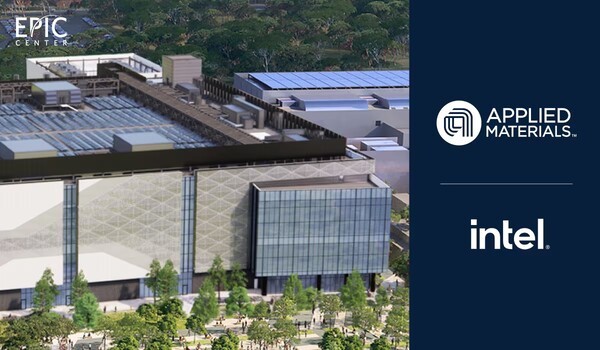
To this end, the two companies will combine their research capabilities and use Applied's EPIC (Equipment and Process Innovation and Commercialization) Center in Silicon Valley and Intel's R&D campus in Hillsboro, Oregon. The goal is to shorten the time required from R&D to commercialization in core advanced semiconductor technologies for AI computing.
The focus of this collaboration is to address rising demand for AI computing. The two companies also centered the partnership on simultaneously advancing performance, power efficiency, and packaging technologies.
The two companies will expand cooperation on next-generation materials for advanced logic nodes for AI workloads, and will also broaden cooperation on process technology and device architecture. The collaboration will place emphasis on further scaling interconnects, and the two companies will jointly push ahead with technological innovation across FEOL (Front-End-of-Line) processes and BEOL (Back-End-of-Line) processes.
The collaboration also includes advanced packaging, and the companies will pursue development of 3D stacking technology based on Intel Foveros. Through this, they aim to support high-performance computing platforms for accelerating agentic AI workloads and to enable higher interconnect density, improved power delivery, and enhanced thermal performance.
The purpose of the collaboration is to address device scaling challenges stemming from deepening semiconductor miniaturization. The two companies have continued collaborating for decades to advance semiconductor roadmaps, and going forward they plan to strengthen joint R&D around the EPIC Center.
Gary Dickerson, chairman and CEO of Applied Materials, said Applied Materials and Intel have maintained close cooperation for decades, advancing semiconductor roadmaps and pushing the limits of materials engineering. He said teams from both companies are participating jointly at the EPIC Center and that the collaboration will further strengthen the partnership.
Gary Dickerson said the joint work at the EPIC Center will accelerate transistor, interconnect, and packaging innovations tied to the future of AI computing. He said EPIC Center collaboration provides the foundation for speeding up these core innovations.
Lip-Bu Tan, Intel CEO, said that as AI computing demand increases, major advances in performance, power efficiency, and packaging are required. He said Intel is focused on realizing these innovations and is working closely with partners across the ecosystem, with Applied Materials as an important partner. He added that he expects expanded collaboration at the EPIC Center to speed up the path from research in the United States to mass production.
Prabu Raja, president of Applied Materials' Semiconductor Products Group (SPG), said the semiconductor manufacturing roadmap is becoming more complex as process nodes advance. He explained that deeper collaboration across R&D and manufacturing is needed to accelerate innovation in semiconductor devices, interconnects, and packaging.
In this context, Naga Chandrasekaran, executive vice president and CTOO of Intel and head of Intel Foundry, said accelerating R&D in step with the rapid expansion of AI infrastructure is important. He explained that the technology, advanced manufacturing capabilities, and foundry services customers expect from Intel Foundry are linked to R&D acceleration.
Naga Chandrasekaran said Applied Materials' new EPIC Center provides a closer and faster collaboration environment for teams from both companies. He said the EPIC Center will help accelerate materials development and process innovation. Applied Materials' new EPIC Center in Silicon Valley is scheduled to be ready for operation later this year and was designed to shorten the commercialization timeline for innovative technologies across the full path from early-stage research to large-scale mass production.
In a secure collaboration environment, chip manufacturers can gain early access to Applied's R&D portfolio and secure a faster learning cycle, and this early access and rapid learning cycle can accelerate the transition of next-generation technologies to mass production, making it possible to bring those technologies to mass production sooner.
Source: TECHWORLD · Park Kyu-chan
Original: https://www.epnc.co.kr/news/articleView.html?idxno=407852
References
This article was produced with the help of an automated content generation algorithm.
Source: TECHWORLD
View originalThis article was summarized and organized by BizCrush based on the original article from TECHWORLD. For exact quotations and full details, please refer to the original article.