Applied and Besi Expand Joint Development of Advanced Packaging Technologies for the AI Era
TECHWORLD ·
✦ AI Summary
Applied Materials announced on the 2nd that it will expand its strategic collaboration with Besi in advanced packaging and interconnect technologies.
In the expansion, Besi will join Applied's EPIC Center as an innovation partner, and the two companies will broaden the scope of joint innovation beyond hybrid bonding to new interconnect architectures and applications.
Building on the joint CoE and Kinex development in 2020, the two companies plan to expand collaboration to include hybrid bonding, TCB scaling, die-on-panel integration, and interconnect technologies for next-generation AI and photonics systems.
Applied Materials announced on the 2nd that it will expand its strategic collaboration with Besi (BE Semiconductor Industries) in advanced packaging and interconnect technologies. The expanded partnership builds on a joint development program that began in 2020.
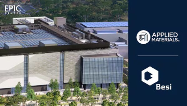
Under the expansion, Besi will join Applied Materials' EPIC (Equipment and Process Innovation and Commercialization) Center as an innovation partner. Through this, the two companies will work to broaden the scope of joint innovation beyond hybrid bonding to new interconnect architectures and applications.
The accelerated buildout of AI infrastructure was cited as the backdrop for the expanded collaboration. As a result, the need to increase the integration density and performance of chips used in AI systems is also growing.
At the same time, the importance of chip-to-chip and chip-to-package interconnect technologies is also increasing. Against this backdrop, Applied Materials announced the expansion of its strategic collaboration with Besi.
The two companies established a joint CoE (Center of Excellence) in 2020 at Applied's Advanced Packaging Development Center in Singapore. In the joint CoE, Applied's etch, planarization, deposition, wafer cleaning, metrology, inspection, and particle defect control technologies were combined with Besi's die placement, interconnect, and assembly technologies. As a result of that joint development, they developed 'Kinex,' the industry's first die-to-wafer hybrid bonding integrated system.
The collaboration at the EPIC Center will expand the existing joint development scope. The two companies plan to jointly optimize process and assembly solutions across advanced packaging, from wafer-level hybrid bonding to panel-scale integration. The goal is to help customers adopt new interconnect technologies earlier.
To this end, Besi engineers will work with Applied's team at the EPIC Center. Areas of expanded joint development include hybrid bonding, thermal compression bonding (TCB) scaling, die-on-panel integration, and interconnect technologies for next-generation AI and photonics systems.
Gary Dickerson, chairman and CEO of Applied Materials, said Besi has been a long-trusted partner since the two companies began joint development of next-generation hybrid bonding solutions. Richard Blickman, CEO and chairman of the management board of Besi, said the CoE jointly operated with Applied in Singapore became the foundation for Besi's hybrid bonding roadmap.
Besi has joined Applied's EPIC Center as an innovation partner. With Besi's addition, the scope of collaboration will expand to encompass the full range of interconnect technologies needed to scale customers' AI systems.
Gary Dickerson said that pursuing collaboration at the Applied EPIC Center allows the two companies to identify the direction of their technology roadmaps early and enables joint optimization of the entire packaging flow. Richard Blickman said that joining the Applied EPIC Center as an innovation partner is a natural next step.
The focus of this collaboration is to treat interconnect and advanced packaging technologies not as back-end processes separate from front-end manufacturing, but as a continuous manufacturing flow. According to his remarks, the two companies are pursuing interconnect technology development with leading logic, memory, and systems companies, and the goal of this technology is to support TCB scaling, die-on-panel integration, and next-generation AI and photonics systems.
The two companies view advanced packaging not as a simple back-end assembly technology, but as a materials engineering challenge connected to front-end wafer manufacturing. They said this is driven by the expansion of hybrid bonding and panel-level integration technologies, and that this spread requires front-end-level precision, front-end-level cleanliness, and process control capabilities.
Prabu Raja, president of Applied Materials' Semiconductor Products Group, said advanced packaging is a materials engineering challenge that requires front-end wafer-manufacturing-level precision and cleanliness, not a back-end assembly stage. He said joint development with Besi engineers is possible in a front-end R&D environment such as the EPIC Center, adding that this allows the technologies to be handled as a connected flow rather than fragmented individual processes.
He added that this approach will allow the two companies' customers to use jointly optimized solutions earlier. He also said it could shorten the time from development to high-volume production.
Applied and Besi said they plan to expand their collaboration to respond to the increasing integration density of AI semiconductors and accelerate development of advanced packaging technologies on that basis. The two companies said they plan to expand the scope of joint development, with the expansion covering hybrid bonding, panel-level integration, and next-generation interconnects.
Source: TECHWORLD · Park Gyu-chan
Original: https://www.epnc.co.kr/news/articleView.html?idxno=407715
References
This article was produced with the help of an automated content generation algorithm.
Source: TECHWORLD
View originalThis article was summarized and organized by BizCrush based on the original article from TECHWORLD. For exact quotations and full details, please refer to the original article.