Applied Materials and Kioxia to Jointly Develop Next-Gen AI Memory at EPIC Center
TECHWORLD ·
✦ AI Summary
Applied Materials announced on the 30th that it will pursue joint development cooperation with Kioxia on next-generation AI memory technologies. The two companies will jointly research advanced memory cell and structure formation, multi-chip stacking architectures, advanced packaging, and new materials engineering approaches. The partnership aims to develop high-performance, highly integrated memory architectures for AI applications and commercialize next-generation memory technologies based on Applied’s EPIC Center in Silicon Valley.
Applied Materials announced on the 30th that it will pursue joint development cooperation with Kioxia on next-generation AI memory technologies. The partnership aims to develop next-generation memory technologies required in the AI era. Kioxia, a global flash memory and SSD company, has joined Applied’s EPIC Center in Silicon Valley as an innovation partner. EPIC stands for Equipment and Process Innovation and Commercialization.
Under the partnership, the two companies will jointly research advanced memory cell and structure formation, multi-chip stacking architectures, advanced packaging, and new materials engineering approaches. The research will include advanced memory cell and structure formation technologies. Based on this, the companies aim to develop high-performance, highly integrated memory architectures for AI applications.
The two companies also presented next-generation multi-chip stacking technology as a joint development target. The technology is intended to improve memory capacity and performance within a limited form factor. The joint research areas of multi-chip stacking architectures, advanced packaging, and new materials engineering approaches will also be pursued in line with this direction.
Through the partnership, the two companies plan to improve memory density and performance for AI applications. They also plan to accelerate the commercialization of next-generation memory technologies. Applied Materials said the partnership formalized its collaboration with Kioxia on next-generation AI memory development.
The two companies will cooperate in advanced packaging for stacked memory and develop technologies to improve the integration density and interconnect performance of complex multi-die memory solutions. The partnership is being pursued with large-scale mass production in mind, while also exploring materials engineering innovation that could enable next-generation memory structures.
Gary Dickerson, chairman and CEO of Applied Materials, said memory solutions for AI infrastructure require breakthrough levels of density, wider bandwidth, and improved energy efficiency. He said the company has established a strong partnership at the EPIC Center aimed at redefining the possibilities of next-generation memory by combining Kioxia’s memory technology expertise with Applied’s materials engineering innovation.
Hiroo Ota, president and CEO of Kioxia, said the potential of memory depends on pushing the limits of materials and process innovation. He added that the collaboration with Applied Materials shows a shared commitment to pursuing memory innovation.
He said he hoped the companies would jointly achieve advanced technological innovation at the EPIC Center. Prabu Raja, president of Applied Materials’ Semiconductor Products Group (SPG), said memory is at the center of the AI innovation roadmap, and explained that improving memory density requires managing cost and complexity as well as innovation across materials, equipment, and process technologies.
Minori Kajimoto, head of advanced memory development at Kioxia, said the companies have secured an environment at the EPIC Center where they can work with Applied Materials to solve next-generation memory challenges. He added that the companies will pursue close collaboration among their top innovation talent and aim to achieve a new level of integration density and performance for AI computing.
Kajimoto also expressed his willingness to accelerate the commercialization of next-generation memory and packaging technology innovation. Representatives from the two companies said that through cooperation at the EPIC Center, they will solve technical challenges in memory and packaging and pursue improvements in integration density and performance needed for AI computing.
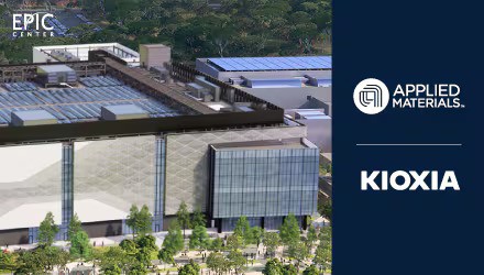
The Applied Materials EPIC Center, which underpins this collaboration, is a approximately USD 5 billion advanced semiconductor equipment R&D facility being built in Silicon Valley. The company described it as the largest investment in advanced semiconductor equipment R&D in U.S. history, and said the EPIC Center is scheduled to be ready for operation later this year.
The EPIC Center was designed to shorten the time required to commercialize technologies from the early research stage to large-scale mass production. To that end, chipmakers can gain early access to Applied’s R&D portfolio in a secure collaborative environment and, through rapid learning cycles, transfer next-generation technologies to large-scale mass production.
Source: TECHWORLD · Park Gyu-chan
Original: https://www.epnc.co.kr/news/articleView.html?idxno=407522
References
This article was produced with the help of an automated content generation algorithm.
Source: TECHWORLD
View originalThis article was summarized and organized by BizCrush based on the original article from TECHWORLD. For exact quotations and full details, please refer to the original article.