Applied: “AI Chips Are No Longer a Chip-by-Chip Battle ... It’s a Battle of Systems” — System Integration Beyond HBM
TECHWORLD ·
✦ AI Summary
Applied Materials said advanced packaging and system integration are key to semiconductor competitiveness in the AI era.
It explained that AI semiconductor performance is becoming more dependent on data movement between memory and compute chips, power efficiency, and system integration than on single-chip computing performance.
To that end, it presented a strategy and related technology roadmap for connecting DRAM, HBM, and logic chips into one system.
Applied Materials said advanced packaging and system integration are the key competitive advantages for semiconductors in the AI era. It explained that efforts to improve AI accelerator performance cannot rely solely on shrinking individual chips, and that competition in AI semiconductors is shifting from the chip level to the system level. To that end, it said DRAM, HBM, and logic chips need to be connected as one system, with the goal of simultaneously improving data movement efficiency and power efficiency.
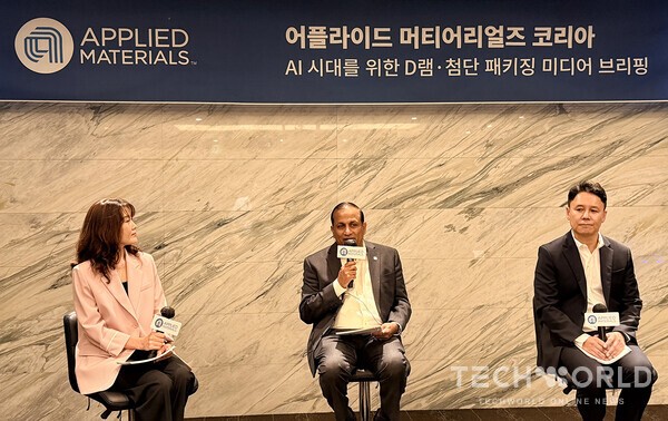
Applied Materials held a media briefing for local media at Oakwood at COEX in Seoul on the 31st under the theme, "Industry Trends and Technology Roadmap in the AI Era." The briefing covered changes in the AI semiconductor market, next-generation memory, and advanced packaging technology strategies. Mukund Srinivasan, executive vice president of the Applied Materials Group, and Park Kwang-sun, president of Materials Korea, attended.
The event was titled, "AI Memory Scaling: From DRAM to HBM to System Integration." It focused on changes in the memory industry driven by the spread of AI and on Applied Materials' materials engineering and advanced packaging technology roadmap. Applied Materials introduced an advanced packaging strategy and related technology roadmap for connecting DRAM, HBM, and logic chips together.
In his welcome remarks, President Park said the semiconductor industry has grown over the past year and that the importance of advanced packaging has increased. He said the role of advanced packaging is changing beyond the limits of single-chip performance into a strategic technology for overall integration and efficiency improvement.
Park said the purpose of the event was to discuss packaging solutions for integrating logic chips with major Korean customers. He also said that a key task in the AI era is not only improving the performance of individual semiconductors, but also connecting multiple chips and integrating them into one system.
Applied said that while model size and data throughput continue to increase in AI computing, improvements in bandwidth, memory capacity, and energy efficiency are not keeping pace with AI demand. As a result, it said AI computing is facing the challenge of the "Memory Wall," and that a rapid expansion of advanced packaging technologies, including HBM and 3D stacking, is needed as a solution.
The factors determining AI semiconductor performance are expanding from the computing capability of a single chip to data movement between memory and compute chips, power efficiency, and system integration. Executive Vice President Srinivasan said processor performance continues to improve, but if memory storage and supply performance cannot keep up, overall system performance is constrained.
Srinivasan said that DRAM speed and density must therefore improve. He added that the importance of vertical HBM stacking is growing, and that the importance of single-package integration technology for logic and memory chips is also expanding.
Applied presented four strategic pillars in response: DRAM device innovation, HBM stacking, system-level integration, and co-innovation with customers. Among them, it is pushing to improve memory speed and power efficiency by applying leading-edge logic verification transistor, interconnect, and materials technologies to DRAM.
It is also using TSV, micro-bumps, hybrid bonding, thermal management, and warpage control technologies. Through these, it is pushing to increase the number of stacked HBM layers.
The direction of semiconductor integration is moving toward an optimized systemization of memory, compute, and connectivity through 2.5D and 3D packaging, co-packaged optics (CPO), and panel interposer use. In line with this trend, Applied unveiled a new system in June to support the implementation of 3D architectures for AI chips.
The equipment unveiled this time includes CMP, deposition, and electron-beam metrology systems. Based on these, Applied is strengthening its portfolio across DRAM and advanced packaging.
Another key trend highlighted was extending logic-class materials engineering technologies to DRAM. Srinivasan said the DRAM technology roadmap is changing as AI demand expands, and that as the difficulty of shrinking DRAM increases, expanding the use of EUV is becoming important.
Srinivasan also said it is important to apply leading-edge logic transistor and materials technologies to memory peripheral circuits. As an example, selective epitaxial growth of silicon germanium (SiGe) in the source and drain regions of DRAM peripheral-circuit transistors was cited, and it was explained that this creates channel strain, improving transistor performance and reducing power consumption.
In addition, the expansion of EUV use is expected to increase the number of copper wiring layers. It was explained that this is because more wiring layers are needed to expand the integration of memory cells and peripheral circuits within a single chip.
While peripheral-circuit transistor structures are changing inside DRAM, Applied presented a direction for applying logic-class transistor technology to DRAM. The effects of applying logic-class transistor technology were cited as performance improvement and power-efficiency improvement.
At the same time, HBM is positioning itself as a core memory technology supporting AI accelerator performance. HBM is implemented through a structure in which multiple DRAM dies are vertically stacked using TSV, and this implementation characteristic enables high bandwidth.
However, because there is a required area for TSV formation, DRAM dies for HBM may become larger than those for conventional DRAM. As a result, producing the same capacity requires more wafers for HBM.
Regarding this, Executive Vice President Srinivasan stressed that rising HBM demand will not only increase demand for front-end DRAM equipment, but will also lead to higher demand across advanced packaging process equipment, including TSV, thinning, bonding, CMP, metrology and inspection, and thermal management.
Accordingly, Applied projected more than 70% growth in advanced packaging revenue in 2026. It is also strengthening its panel-level technology portfolio for implementing large AI accelerator packages, and is pursuing acquisition of panel-level electrochemical deposition (ECD) technology through the acquisition of NEXX.
As HBM stacking becomes more advanced, the importance of interconnect technology for chip-to-chip connections is rising. Chip-to-chip connection technology has evolved from wire bonding to flip chip, micro-bumps, TSV-based thermocompression bonding (TCB), and hybrid bonding.
Hybrid bonding removes bumps and directly bonds copper. This reduces the pitch for chip-to-chip connections and enables high I/O density.
Applied said hybrid bonding makes it possible to achieve I/O densities of up to 1 million per square millimeter. It also said the energy required for data transmission can be significantly reduced.
Applied unveiled its die-to-wafer hybrid bonding system, "Kinex," last year. The purpose was to strengthen advanced packaging technology that supports the production of high-performance, low-power AI logic and memory chips.
CPO is drawing attention as a next-generation technology. CPO uses optical data transmission, and its data transmission method is optical signals. It is being discussed as a package-level integration method for electronic and optical chips, with the goal of surpassing the limits of electrical interconnects.
The growing interest in CPO, which uses optical signals, is being driven by the surge in data processed by AI data centers. At the same time, CPO is attracting attention for its potential to deliver higher bandwidth and lower energy consumption for data movement.
At the same time, larger-area requirements are increasing for interposers used in large AI accelerators. However, when producing square interposers with conventional 300 mm round silicon wafers, area loss occurs at the wafer edges.
Given these limitations, panel-level packaging technology using large panels is emerging. Panel-level packaging is presented as offering higher productivity and lower costs.
Applied laid out target specifications for panel interposers in stages. The specifications presented were 310 x 310 mm, 510 x 515 mm, and, in the long term, 600 x 600 mm.
To accelerate the commercialization of next-generation AI memory technologies, Applied is expanding joint R&D with customers. President Park said the goal is to speed up the commercialization of next-generation AI memory technologies and to accelerate joint research and development with customers.
Park said the difficulty of scaling memory, HBM stacking, and advanced packaging is increasing. He added that there are limits to optimizing materials, devices, processes, packaging, and systems separately.
Applied is promoting co-innovation with Samsung Electronics and SK hynix through EPIC and ACC Korea. EPIC is short for Equipment and Process Innovation and Commercialization Center, a co-innovation platform involving customers, partners, universities, and research institutes.
EPIC is operated with the goal of collaborating from the earliest stages of technology development and linking research results to mass production. As of the third quarter of fiscal 2026, 11 R&D collaborations were underway at the EPIC center with major chipmakers, universities, and innovation partners.
President Park Kwang-sun said Samsung Electronics and SK hynix are participating as founding partners of EPIC. He added that Applied has signed a long-term R&D partnership with SK hynix to accelerate the development and adoption of next-generation DRAM and HBM, and is pursuing joint research at the Silicon Valley EPIC center.
In Korea, Applied Collaboration Center Korea (ACC Korea) is being established in Osan, and ACC Korea will support joint technology development and mass-production validation for domestic customers. President Park Kwang-sun emphasized the link between the Korea R&D base and the global EPIC center, saying this structure will help shorten the time needed to commercialize next-generation semiconductor technologies.
Within this trend, Applied's AI memory scaling strategy was presented as going beyond simply expanding equipment supply. It includes applying leading-edge logic verification materials engineering technology to DRAM, improving memory bandwidth and capacity through HBM and 3D stacking, and using hybrid bonding, CPO, and panel interposers, with system integration of memory, compute, and connectivity positioned as the core of the strategy.
As the focus of AI semiconductor competition shifts from "faster chips" to "more efficiently connected systems," Applied presented a strategy to strengthen its push into the AI semiconductor market, backed by a materials engineering portfolio spanning DRAM, HBM, advanced packaging, and system integration.
Source: TECHWORLD · Park Kyu-chan
Original: https://www.epnc.co.kr/news/articleView.html?idxno=406278
References
This article was produced with the help of an automated content generation algorithm.
Source: TECHWORLD
View originalThis article was summarized and organized by BizCrush based on the original article from TECHWORLD. For exact quotations and full details, please refer to the original article.