[DigiKey TechForum] Efficient MOSFET Driving Techniques for High-Speed Switching: Push-Pull and Bootstrap Topologies
TECHWORLD · · 2 views
✦ AI Summary
Push-pull driving consists of two MOSFETs or bipolar transistors and alternately raises and lowers the gate voltage.
Its advantages include fast switching speed, high drive capability, and reduced crossover loss, while its disadvantages include the need for precise dead time control and higher cost and control complexity.
Bootstrap driving stores a voltage difference in a capacitor when the low-side MOSFET is ON to drive a high-side N-MOSFET, and it has limitations on high-side conduction time and PWM duty cycle.
The previous article covered the basic driving topologies for low-side and high-side MOSFETs. This is a fundamental aspect of MOSFET driving and something that should be reviewed first.
The switching speed and efficiency of power devices continue to improve. As a result, there are cases where it is difficult to secure performance and reliability with only conventional low-side and high-side driving.
As an alternative to these limitations, the application of advanced driving topologies such as push-pull and bootstrap is proposed. These advanced topologies improve performance and offer a range of advantages in various applications.
This article focuses on push-pull driving and bootstrap driving. It will cover each method’s operating principle, advantages, design considerations, and practical use cases.
Push-pull driving consists of two MOSFETs or bipolar transistors. In this configuration, the two devices operate in complementary opposition.
The function of this push-pull drive is to alternately raise and lower the gate voltage. This helps explain the basic operation of push-pull driving.
This configuration is suitable for the output stage of a gate driver IC.
Example ICs include Microchip TC4420 and TC4429.
This configuration is also suitable for high-frequency, high-current switching drives, and application examples include PWM control and motor control.
One advantage is fast switching speed.
This is based on rapid charging and discharging of the gate capacitance.
Another advantage is high drive capability, with levels exceeding 2A.
Reduced crossover loss is also cited as an advantage.
On the other hand, one drawback is the need for precise dead time control to prevent shoot-through current.
Relatively high cost and complex control are also cited as disadvantages.
In design, care must be taken to prevent shoot-through when designing a push-pull driver. In a push-pull configuration where the two drivers alternate on states, improper dead time can cause the upper and lower drivers to turn on at the same time, creating the possibility of a short circuit.
If the switching speed is excessive, EMI or oscillation may occur. By adjusting the gate resistance value, switching speed can be properly controlled and EMI reduced.
When designing a MOSFET driving circuit, the drive current must be selected to match the MOSFET gate charge and the required switching speed. At the same time, the driver’s current supply capability should be checked to determine whether the gate can be charged and discharged quickly.
In PCB layout, the goal should be to minimize the parasitic inductance and capacitance of the current path. This helps maintain signal integrity and reduce EMI issues.
Half-bridge drivers generally have built-in shoot-through prevention circuitry. However, in some cases it is necessary to secure additional dead time, and this can be implemented by setting constraints on the microcontroller’s PWM signal.
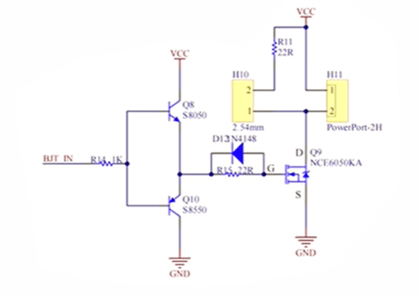
In addition, a limit must be placed on the PWM duty cycle to ensure that the bootstrap capacitor is sufficiently charged. The example below shows a transistor-based low-side push-pull driving circuit.
In this example, 8050, 8550, B772, and D882 can be used. The test power supply is DC 12V, and under this power condition no separate drive voltage is needed.
When the load voltage is higher than the control voltage, the drive voltage needs to be lowered.
This is to prevent the MOSFET’s Vgs from exceeding its allowable range.
For the recommended IC category, bootstrap driving is proposed.
The principle of bootstrap driving is to store a voltage difference in a capacitor when the low-side MOSFET is ON.
The stored voltage is then used to drive the high-side N-MOSFET.
This method is suitable for half-bridge and full-bridge circuits.
Example applications include inverters and motor drives.
The use condition is when the high-side MOSFET’s Vgs must be raised sufficiently.
Advantages include high efficiency from using an N-MOSFET for high-side switching, in addition to low RDS(on).
Another advantage is miniaturization and lower cost.
On the other hand, one drawback is that the high-side MOSFET cannot be kept continuously ON.
Periodic low-side conduction is also required to recharge the bootstrap capacitor, and because time must be allowed for capacitor charging, the PWM duty cycle is also constrained.
This section presents the selection criteria for each component in the bootstrap circuit. Design considerations include the bootstrap capacitor (C_boot), bootstrap diode, and bootstrap resistor (R_boot).
The bootstrap capacitor (C_boot) is used to supply sufficient charge during switching. The selection criterion for C_boot is at least 10 times the high-side MOSFET gate capacitance, and voltage ripple reduction and improved reliability are also considered. Recommended capacitor characteristics are low ESR and low ESL, and the recommended capacitor type is an MLCC.
The bootstrap diode is selected to reduce power loss and improve switching speed. Selection criteria for the diode include low forward voltage drop and fast reverse recovery, and the recommended diode type is a Schottky diode.
The bootstrap resistor (R_boot) is used to limit peak current at startup and protect the diode. The selection criterion for R_boot is to consider charging time and current limiting at the same time, and the design should strike a balance in a way that prevents excessive charging delay and excessive inrush current.
When implementing a bootstrap circuit for high-side MOSFET gate driving, the PCB layout should place the bootstrap capacitor, diode, and driver IC close together to minimize parasitic inductance and resistance. It is also necessary to reduce the loop area of the high-current path to minimize EMI and voltage spikes.
However, there are limitations on conduction time. Because the bootstrap circuit may have limits in maintaining capacitor voltage, it is not suitable when long-duration conduction of the high-side MOSFET is required.
For this reason, isolated driving should be considered in low-frequency or static applications. This is intended to address the limitations of the bootstrap method in conditions that require long-duration conduction.
The example circuit corresponds to a simple high-side MOSFET gate drive circuit for H-bridges for brushed motors or brushless motors, or for a three-phase H-bridge. In this circuit, the bootstrap capacitor C1 supplies the energy required for gate drive, and the gate drive energy is directly delivered by the optocoupler output transistor.
The circuit configuration is common collector.
In this bootstrap-based circuit, the NPN transistor raises the MOSFET gate voltage to the bootstrap voltage.
When the MOSFET is turned off, R2 discharges the gate charge through R4.
At this time, the function of R4 is current-limiting resistance.
Next, the driving topologies to compare are push-pull and bootstrap.
Push-pull is applied to high-frequency switching and digital circuits. Its advantages are high drive current and fast switching speed, while its disadvantage is the need for precise dead time control. The main IC solutions for push-pull are Microchip TC4420 and Microchip TC4429.
Bootstrap is applied to half-bridge and full-bridge circuits and high-side switching. Its advantages are that a separate isolated power supply is unnecessary and the cost is low, while its disadvantages are the limitation on high-side conduction time and the importance of selecting the bootstrap capacitor capacity. The main IC solutions for bootstrap are TI UCC27710 and Infineon EiceDRIVER.
In conclusion, push-pull and bootstrap topologies provide high-speed, high-efficiency MOSFET switching methods.
Push-pull driving is suitable for high-speed control that requires strong gate drive capability. The bootstrap circuit allows an N-MOSFET to be used on the high side without a separate power supply.
These two methods each have advantages and limitations. Therefore, in stable power circuit design, understanding the characteristics of each method and determining when and how to apply them becomes an important factor.
Next, we will look at optically isolated driving methods for high-voltage, complex motor control environments. We will also cover bridge driving methods for high-voltage, complex motor control environments.
The original reference source is DigiKey’s TechForum/Article.
Source: TECHWORLD · Lee Gwang-jae
Original: https://www.epnc.co.kr/news/articleView.html?idxno=407110
References
This article was produced with the help of an automated content generation algorithm.
Source: TECHWORLD
View originalThis article was summarized and organized by BizCrush based on the original article from TECHWORLD. For exact quotations and full details, please refer to the original article.