ON Semiconductor Unveils EPP for AI Data Center Power Innovation
TECHWORLD ·
✦ AI Summary
On the 18th, ON Semiconductor unveiled the Embedded Power Platform (EPP: Embedded Power Platform).
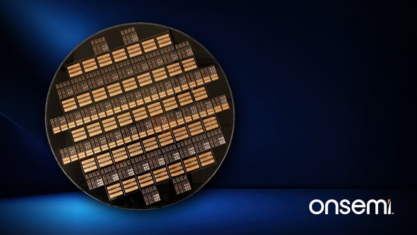
EPP is a scalable platform that integrates electrical, mechanical, and thermal design from the outset and uses the silicon wafer itself as part of the system architecture.
ON Semiconductor said EPP can deliver 3 to 5 times higher power density and cut development time by up to 4 months, and it plans to supply samples to key strategic customers and ecosystem partners in automotive and AI applications starting in 2026.
As ON Semiconductor pushes ahead with power semiconductor innovation targeting the AI infrastructure and electric vehicle markets, it has unveiled a new power system architecture that uses silicon wafers on a package-based basis. On the 18th, ON Semiconductor unveiled the Embedded Power Platform (EPP: Embedded Power Platform).
EPP is a scalable platform that integrates electrical, mechanical, and thermal design from the outset. The platform is aimed at delivering high power density and system performance.
EPP was designed to accelerate development of AI, electrification, and autonomous systems applications. Through this platform, ON Semiconductor presented a structure that helps combine electrical, mechanical, and thermal elements from the earliest stages of design to secure high power density and performance.
Hassane El-Khoury, president and CEO of ON Semiconductor, said semiconductors and packages had traditionally been seen as separate technologies. He explained that EPP changes that mindset by integrating silicon itself as part of the system architecture.
The speaker referred to the common-architecture integration of advanced semiconductor technology, manufacturing, and system-level optimization. As an effect of that integration, the speaker pointed to the possibility of future innovation response and coevolution. The speaker also mentioned the potential to lay the groundwork for AI infrastructure, electrification, and automation.
Next, a new definition of EPP was presented. Compared with the passive outer-shell role of conventional packages, EPP was redefined as an element that directly contributes to system performance. ON Semiconductor's approach is to use the silicon wafer itself as the package.
ON Semiconductor's integration targets are silicon, silicon carbide (SiC), and gallium nitride (GaN). Its implementation takes the form of integration and interconnection of different semiconductor technologies within a wafer-level architecture. FETs, drivers, and controllers can be embedded in the package. By embedding multiple devices in a single package, it becomes possible to comprehensively optimize electrical, thermal, and mechanical performance.
As a result, co-design of power systems becomes possible. This co-design approach evaluates and optimizes electrical, thermal, and mechanical characteristics simultaneously from the early design stage. The co-design effect reduces complexity in the development process and eases the burden of late-stage design changes.
ON Semiconductor is moving to apply EPP to its standard 12-inch silicon wafer manufacturing capabilities. The company plans to apply proven semiconductor design tools, wafer-scale manufacturing technology, and advanced simulation capabilities to power system integration. Through this, it plans to pursue performance improvements and development innovation.
The goal of EPP is to transform the sequential design method of conventional power systems into an integrated platform. On this integrated platform, co-design, simulation, and optimization are possible.
ON Semiconductor said this approach can deliver 3 to 5 times higher power density than conventional methods, depending on the application, and cut development time by up to 4 months. Accordingly, it is expected to improve thermal performance, enhance heat dissipation, reduce power loss through lower parasitic inductance, improve device control performance, and enable higher switching frequencies.
These characteristics are expected to be used as a solution in the AI infrastructure sector to meet rising power demands for AI racks. In an early EPP-based solid-state circuit breaker design, size was reduced by 50% and temperature by 20% compared with the existing design.
ON Semiconductor said EPP reduces the space needed for packaging and enables heat dissipation across the entire surface area. It said this makes it possible to build more compact power systems based on EPP.
ON Semiconductor said these characteristics could lead to higher power density in AI data centers. It also said they could ease cooling constraints and space constraints in AI data centers.
In the electric vehicle sector, traction inverters were identified as a key application. The design goal of EPP is up to 4 times higher power density than conventional methods and 15% lower power loss than conventional methods, the company said.
ON Semiconductor said EPP supports a common inverter platform for a range of power ratings targeting mass-market to premium vehicles. It said this could help automakers reduce R&D costs and manufacturing costs, shorten verification cycles, and shorten development cycles.
Subaru also joined as an early EPP collaboration partner. ON Semiconductor and Subaru are evaluating ways to apply EPP to future electrified vehicle architectures, and the sample supply timing is 2026.
During the collaboration, Subaru received engineering samples early, simulation models early, and technical expertise early. Based on this, the two companies plan to explore ways to improve vehicle performance, ways to increase development efficiency, and ways to accelerate innovation.
ON Semiconductor emphasized that the importance of power management technology is increasing in AI infrastructure, electrified transportation, and industrial automation. As computing performance expands and EV electrification progresses at the same time, there is a growing need to increase power delivery within limited space, and the burden of power management within limited space is also increasing, the company said. EPP aims to address power, thermal, and spatial constraints from a system design perspective.
Accordingly, ON Semiconductor plans to supply EPP samples starting in 2026. The sample supply targets are key strategic customers and ecosystem partners in the automotive and AI applications sectors.
Source: TECHWORLD · Park Gyu-chan
Original: https://www.epnc.co.kr/news/articleView.html?idxno=407119
References
This article was produced with the help of an automated content generation algorithm.
Source: TECHWORLD
View originalThis article was summarized and organized by BizCrush based on the original article from TECHWORLD. For exact quotations and full details, please refer to the original article.