KAIST Develops Next-Gen AI Chip Technology That Lets Different Semiconductors Conduct Better
TECHWORLD ·
✦ AI Summary
KAIST Professor Seo Jun-ki's research team announced on the 16th that it had developed a new materials technology called the "Universal van der Waals Tunneling Injector" for supplying electricity to ultra-thin semiconductors just a few atoms thick.
The technology aims to reduce the problem of needing different electrodes by injecting charge into both p-type and n-type semiconductors with a single material, tin diselenide (SnSe₂).
The research team said the p-type WSe₂ transistor's maximum drive current increased by more than 1,000 times compared with conventional nickel-electrode devices, and the n-type MoS₂ transistor recorded an on/off current ratio of more than 1 billion (10⁹).
KAIST's research team led by Professor Seo Jun-ki of the Department of Bio and Chemical Engineering announced on the 16th that it had developed a new materials technology called the "Universal van der Waals Tunneling Injector" to smoothly supply electricity to ultra-thin semiconductors just a few atoms thick. The development was carried out in a joint study with Yonsei University, the Beijing Computational Science Research Center in China, the Korea Institute of Science and Technology (KIST), Ulsan National Institute of Science and Technology (UNIST), and researchers from Samsung Electronics.
The technology is focused on reducing the limits of how electricity is injected into ultra-thin semiconductors. Previously, different types of semiconductors required different electrodes, but the new technology can inject charge into both p-type and n-type semiconductors with a single material, raising expectations that it will improve the miniaturization potential and 3D integration potential of next-generation AI and low-power semiconductors.
The research team implemented a technology using a single material, tin diselenide (SnSe₂). The technology is designed to effectively supply electricity to two different ultra-thin semiconductors.
A transistor is a tiny switch that controls the flow of electricity. Transistors are divided into n-type, in which electrons move, and p-type, in which holes move. In actual semiconductor chips, the CMOS (complementary metal-oxide semiconductor) structure is widely used. CMOS is a combined structure of the two types of transistors.
Recently, 2D semiconductors have drawn attention as candidates for next-generation devices. 2D semiconductors are only a few atoms thick. Using their ultra-thin characteristics makes it possible to stack semiconductor devices in multiple layers. As a result, transistor density within the same area can increase.
However, the conventional method directly connected metal electrodes. This approach could damage ultra-thin semiconductors during manufacturing. There was also the possibility of barriers that would hinder charge transfer. p-type and n-type semiconductors have different charge-injection conditions. For this reason, conventional approaches required different electrode materials for p-type and n-type semiconductors.
To reduce damage and contact-surface issues that occur during contact with ultra-thin semiconductors, the research team used tin diselenide. Rather than forming strong chemical bonds with other semiconductors, SnSe₂ makes contact based on van der Waals forces, reducing damage to ultra-thin semiconductors and forming a smooth contact surface.
SnSe₂ implemented different charge-transfer mechanisms depending on the type of semiconductor it was connected to. In p-type tungsten diselenide (WSe₂), interband tunneling was applied, and charge transfer in p-type WSe₂ occurred through tunneling rather than by directly overcoming a high barrier. In n-type molybdenum disulfide (MoS₂), an electric field was used to thin the barrier and induce tunneling.
As a result, the research team confirmed the possibility of integrating the structure, which had required separate electrodes for n-type and p-type semiconductors, into a single material. In addition, the p-type WSe₂ transistor using SnSe₂ saw its maximum drive current increase by more than 1,000 times compared with conventional nickel-electrode devices.
The improved switching performance of the n-type MoS₂ transistor led to better control of current on and off. This transistor recorded an on/off current ratio of more than 1 billion (10⁹), showing smooth current flow in the on state and effective current blocking in the off state.
Based on this, the research team fabricated a CMOS inverter combining n-type and p-type transistors and confirmed that it operated stably even under repeated electrical signals. The significance of this study lies in moving away from the conventional approach of designing separate electrodes for each semiconductor type and solving the charge-injection problem with a single material.
If large-area manufacturing technology is secured in the future, it could open up possibilities for the development of 3D semiconductor technology, and if integration process technology is secured, it could also make it possible to stack 2D semiconductors that are only atomic layers thick. This could allow more transistors to be integrated in the same space, reduce power consumption, and improve computing performance. Such applications are expected in next-generation AI semiconductors and ultra-low-power electronic devices.
Professor Seo Jun-ki of KAIST said that this study suggested the possibility of solving a key hurdle in charge access for monolayer 2D semiconductors with a single type of material. He added that if direct growth and large-area process technologies are further developed, commercialization of low-power 2D CMOS integrated circuits is expected to accelerate.
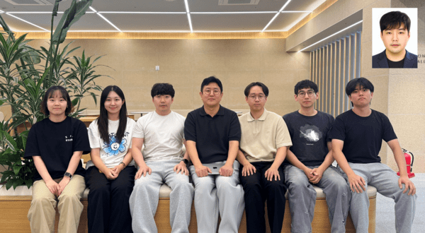
In this study, KAIST doctoral student Jo Han-bin participated as the first author, while Professor Ko Gyeong-min of Yonsei University and Professor Seo Jun-ki of KAIST served as co-corresponding authors. The results were published online in the international journal "Advanced Materials" on August 12, and the research was conducted with support from Samsung Electronics' New Faculty Industry-Academia Research Program, the Ministry of Science and ICT and the National Research Foundation of Korea's Excellent Young Researcher Program, and the Ministry of Science and ICT and the National Research Foundation of Korea's Pioneer Research Program.
Source: TECHWORLD · Park Kyu-chan
Original: https://www.epnc.co.kr/news/articleView.html?idxno=406999
References
This article was produced with the help of an automated content generation algorithm.
Source: TECHWORLD
View originalThis article was summarized and organized by BizCrush based on the original article from TECHWORLD. For exact quotations and full details, please refer to the original article.