MOSFET Drive Methods for Power Switching and Control
TECHWORLD ·
✦ AI Summary
MOSFETs offer the advantages of fast switching speed, high efficiency, and low conduction loss in power electronics and switching control.
Low-side drive places an N-channel MOSFET between the load and ground, directly controls the gate with an MCU or driver output voltage, and can be applied to LED dimming, motor starting, switch control, power management, and buck converter PWM control.
High-side drive places the MOSFET between the power supply and the load, is used for battery positive-terminal switching and H-bridge, half-bridge, and full-bridge high-side control, and may require a bootstrap circuit or an isolated driver.
MOSFET is short for Metal-Oxide-Semiconductor Field-Effect Transistor. This device is a semiconductor component widely used in modern electronic circuits.
In power electronics and switching control, MOSFETs offer the advantages of fast switching speed, high efficiency, and low conduction loss. These characteristics make them widely used in the field.
However, to realize a MOSFET's performance, it must be driven in a way that matches its position in the circuit and the system's requirements. The drive method is determined according to those conditions.
Among the various drive methods, low-side and high-side configurations are used for general power control such as DC-DC converters, LED dimming devices, and battery-powered systems. These methods are used in general-purpose power control.
In low-side drive, the N-channel MOSFET (N-MOSFET) is placed between the load and ground. In terms of position, the load is at the top and the MOSFET is at the bottom.
In low-side drive, the gate is directly controlled by an MCU or the driver output voltage. This establishes the control structure of low-side drive.
This method can be applied to LED dimming, motor starting, switch control, and power management. It is also suitable for PWM control such as in buck converters.
Its advantages include direct control by the MCU and a simple drive circuit. It also offers fast switching speed, low cost for N-MOSFETs, and low on-resistance (RDS(on)) for N-MOSFETs.
On the other hand, this method has the limitation that current spikes can occur on the ground side. As a result, signal quality may deteriorate.
To address these issues, the ground must be separated and filtering is also necessary. In addition, this method is unsuitable for high-side power switching.
Accordingly, proper MOSFET selection is necessary in design. Criteria include a MOSFET with a gate threshold voltage (Vth) lower than the drive voltage and a MOSFET with low on-resistance to reduce power loss and heat generation. Drive voltage and current must also be taken into account, and sufficient drive voltage to fully turn on the MOSFET must be secured.
When driving a MOSFET, an appropriate gate resistor is needed for stability and noise suppression. A gate resistor can be used to adjust the MOSFET switching speed, reduce EMI, and suppress unnecessary gate voltage oscillation.
A gate pull-down resistor must also be connected. When the driver is off, the pull-down resistor must keep the MOSFET off, prevent the gate from floating, and stop unintended turn-on of the MOSFET.
PCB layout and ground design also need to be optimized. To reduce EMI, the loop area must be minimized, and the grounds of the driver and power MOSFET must be connected stably to prevent problems caused by voltage differences between grounds.
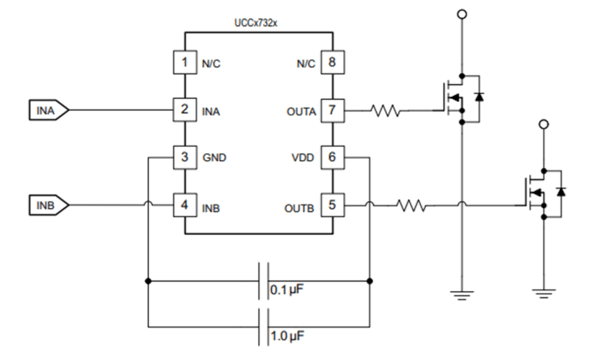
In addition, the TI UCC27324 high-speed dual MOSFET driver is used in circuits that require high-speed switching. The TI UCC27324 provides up to 4 A peak source and sink current, and paralleling the output stages can improve the drive capability of a single channel.
Using the recommended PCB layout for the TI UCC27324DR as an example, specific placement methods for reducing loop area can be seen. The common principle is to minimize the loop area between the signal path and the return path as much as possible.
The gate drive pattern and return pattern are placed on opposite sides of a 2-layer PCB, with an overlapping top-and-bottom design. The gate drive pattern is shown in red and includes a series gate resistor, while the return pattern is shown in blue.
Two DC bypass capacitors are used in parallel. The purpose of using two capacitors is to maintain low impedance across a wide frequency range, and the smaller, closer capacitor serves to handle high-frequency transients.
Two vias are used. The purpose of the two vias is to secure a low-impedance path, thereby minimizing the parasitic inductance of the return loop.
In this way, pattern overlap, close parallel placement of bypass capacitors, and the use of two vias are all connected to reducing the loop between the signal path and the return path. Reducing loop area is a key design element for lowering EMI in high-speed switching environments.
As a technical tip, loop area is closely related to antenna theory in RF design. As loop area increases, it acts like an antenna and EMI emissions increase; therefore, reducing loop area in PCB layout is one of the effective ways to suppress radiated emissions.
In high-side drive, the MOSFET is placed between the power supply and the load. In positional terms, the MOSFET is at the top and the load is at the bottom. In general, a P-channel MOSFET (P-MOSFET) is selected. As an alternative configuration, a bootstrap driver and an N-MOSFET combination are used.
This method is applied to battery positive-terminal switching. It is also applied to power switch control in power management families. In other words, it is used as a form of power switch control.
Its use is also broad in bridge circuits. It is applied to H-bridge high-side control, half-bridge high-side control, and full-bridge high-side control.
The advantage of high-side drive is that it enables control on the positive side of the power supply. When turned off, the load's power supply is cut, improving safety. It is also suitable for lithium battery switching and for reverse polarity protection.
However, the commonly used P-channel MOSFET (P-MOSFET) has limitations. A P-MOSFET has high on-resistance. The performance of a P-MOSFET is also somewhat lower.
When applying an N-MOSFET to high-side drive, additional circuitry may be required. A bootstrap circuit may be needed, and a charge pump may also be needed. For this reason, high-side drive has a more complex drive circuit than low-side drive.
When designing a high-side drive circuit, the drive voltage requirements should be checked first. Because the source voltage of a high-side N-MOSFET rises according to the load voltage, the starting point of the design is securing a drive voltage that can produce sufficient gate-to-source voltage.
The condition for a MOSFET to turn on fully is for the gate voltage to be about 10 V higher than the source voltage. A bootstrap circuit is commonly used as a means of securing this required high-side drive voltage.
However, the bootstrap capacitor must be charged while the MOSFET is off. For this reason, the bootstrap method is unsuitable for long-duration continuous on operation of a MOSFET.
Therefore, when long-duration operation is required or high reliability is demanded, isolated drive should be considered. Examples of isolated drive methods include optocouplers, transformers, and capacitive isolation, and isolated drive methods can secure a stable high-side drive voltage. Protection functions for preventing device damage can also be applied, including overvoltage protection, UVLO, and short-circuit protection.
PCB layout also needs optimization. During the design process, parasitic inductance should be minimized, and parasitic capacitance should also be minimized. This is to maintain signal integrity and to prevent layout-induced EMI.
Along with this, the onsemi FAN73711 high-side gate driver is introduced. The onsemi FAN73711 can operate with a 3.3V control signal and can also operate with a 5V control signal.
The onsemi FAN73711 has a built-in bootstrap function. It also provides UVLO and short-circuit protection.
Among MOSFET drive methods, low-side drive is used for single-channel switching and for low-voltage circuits. Examples of applications include buck converters, LED dimming, and power switches.
The advantages of low-side drive include a simple gate drive circuit and low cost. It also enables fast switching based on the use of N-MOSFETs and is compatible with logic-level signals.
On the other hand, low-side drive has the limitation that positive-side power supply switching is not possible. Ground-side current spikes may occur, and these ground-side current spikes may also affect signal integrity. Representative IC solutions include TI UCCx732x and Microchip MIC4422.
High-side drive is used for high-side load control, battery switching, and motor drive (half-bridge/full-bridge) applications. The advantage of high-side drive is that it enables control on the positive side of the power supply. It can also improve safety by cutting load power when off, and it is suitable for high-voltage switching.
On the other hand, high-side drive has the disadvantage that it requires a bootstrap circuit or an isolated driver. A P-MOSFET has high on-resistance, and drive voltage design is also complex. Example products for high-side drive include Infineon IRS2007 and onsemi FAN73711.
Choosing the proper MOSFET drive method is important for implementing a stable and efficient power control system. Low-side and high-side drive are practical options for low-power and mid-power applications.
If cost matters, ease of implementation matters, and logic-level compatibility matters, low-side drive is suitable. On the other hand, if positive power-line switching is required, high-side drive is suitable.
High-side drive is also suitable for battery-powered systems. It is also suitable when safe load disconnection is required.
If the appropriate components and design methods are applied, these basic drive methods can serve as the foundation for a wide range of electronic system designs.
This information can be found by referring to DigiKey's TechForum/Article.
Source: TECHWORLD · Lee Gwang-jae
Original: https://www.epnc.co.kr/news/articleView.html?idxno=406704
References
This article was produced with the help of an automated content generation algorithm.
Source: TECHWORLD
View originalThis article was summarized and organized by BizCrush based on the original article from TECHWORLD. For exact quotations and full details, please refer to the original article.