Samsung Fab Operations Know-How to Spread to 14 Public Nanofabs
IT DAILY ·
✦ AI Summary
Based on the operational efficiency and improvement cases carried out at POSTECH’s Nano Convergence Technology Institute (NINT), Samsung Electronics will spread fab operation know-how to 14 public nanofabs nationwide.
The Ministry of Science and ICT and Samsung Electronics' DS division's Win-Win Cooperation Center held a results report session at POSTECH’s Nano Convergence Technology Institute in Pohang on the 11th and shared the results of a six-month public nanofab operational efficiency consulting project carried out from March through August.
During the consulting, the team inspected safety and environmental management, site management, equipment operation and equipment maintenance, checked chemical storage, fire protection facilities, leaks and piping, and then applied the 5S3Jung principles to strengthen the foundations for safety, cleanliness, equipment reliability and process service response.
Based on the operational efficiency and improvement cases carried out at POSTECH’s Nano Convergence Technology Institute (NINT), Samsung Electronics will spread the fab operation know-how it has accumulated on semiconductor manufacturing lines to 14 public nanofabs nationwide. The target of this rollout is semiconductor research and development (R&D) and demonstration infrastructure aimed at raising the operating level of public nanofabs, and the company will share with other public fabs the safety, cleanliness and equipment reliability improvements implemented at NINT.
To that end, the Ministry of Science and ICT and Samsung Electronics' Device Solutions (DS) division's Win-Win Cooperation Center held a results report session for the "Samsung Electronics-Nano Convergence Technology Institute Public Nano Fab Operational Efficiency Consulting" at POSTECH’s Nano Convergence Technology Institute in Pohang, North Gyeongsang Province, on the 11th.
Samsung Electronics had transferred its semiconductor fab operation and management know-how to NINT for six months from March through August. During that period, professional consultants inspected the site in person and identified improvement tasks in the areas of safety and environment, site management, equipment operation and equipment maintenance.
At the site, Samsung examined safety and environmental risk factors such as chemical storage, fire protection facilities, leaks and piping. The company applied its "5S3Jung" principles to the manufacturing space. 5S consists of sort, set in order, shine, clean and sustain, while 3Jung consists of proper products, proper quantities and proper placement.
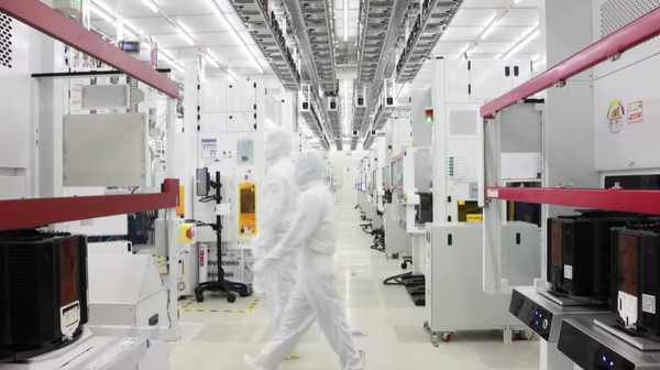
Based on 5S3Jung, NINT strengthened its foundations for safety, cleanliness, equipment reliability and process service response. The photo shows the inside of Samsung Electronics' semiconductor production line at the Pyeongtaek Campus, and the photo was provided by Samsung Electronics.
This project is an example of applying Samsung Electronics' "materials, parts and equipment eye-level consulting" to public research infrastructure. The previous targets of the "materials, parts and equipment eye-level consulting" were materials, parts and equipment (MPE) partners. This time, the scope of manufacturing innovation support was expanded from individual partners to public fabs jointly used by small and medium-sized enterprises and research institutes.
Public nanofabs are shared research infrastructure used by companies, universities and research institutes that have difficulty building their own semiconductor production lines. Public nanofabs are used for process development, prototype production and performance evaluation. The key elements of public nanofab operation are advanced equipment construction, safety management, cleanliness management and stable equipment operation. Operational capability determines the level of actual research and demonstration support.
This consulting was carried out as part of a public fab advancement project promoted by the government and private semiconductor companies. The government and Samsung Electronics plan to sequentially spread the improvement cases identified in this consulting. The targets for expansion are the Korea Nano Technology Institute, the Semiconductor Research Institute at Seoul National University, the Next-Generation Sensor and Semiconductor Research Institute at Daegu Gyeongbuk Institute of Science and Technology (DGIST), and the MPE Technology Center at the Electronics and Telecommunications Research Institute (ETRI).
The government and Samsung Electronics also plan to share best practices with 14 institutions participating in MoaFab, an integrated public nanofab linkage platform. MoaFab is a platform that links equipment and process services across distributed public nanofabs in Korea. In January, the Ministry of Science and ICT expanded the number of MoaFab participating institutions from 6 to 14.
On March 27, 2025, the Ministry of Science and ICT signed a memorandum of understanding with Samsung Electronics, SK hynix and DB HiTek to advance MoaFab functions. The three semiconductor companies plan to cooperate in supporting advanced equipment and in fab operations and technical consulting. They also plan to work together to strengthen R&D, performance evaluation, prototype production and training functions.
The government is seeking to broaden its channels of cooperation with the three semiconductor companies through MoaFab. Yoon Kyung-sook, director of basic and source technology research policy at the Ministry of Science and ICT, said the ministry plans to strengthen public-private cooperation centered on MoaFab and proposed private consulting, the transfer of idle equipment and the use of experienced private-sector experts as cooperation methods. Calls to raise the industrial usability of public fabs have also continued until now.
In line with that direction, the "2026 Semiconductor Packaging Development Policy Forum" was held on the 10th. At the forum, participants said support is needed for tech validation by fabless companies, foundries, OSAT companies and MPE companies, while also calling for support in securing the data needed for mass production conditions. There was also an argument that public testbeds need to be expanded for this purpose, and the Nano Convergence Technology Institute is building a public advanced packaging fab based on 300-mm wafers.
Accordingly, the role of public fabs is also expanding beyond providing research equipment to include process development, prototype production and performance evaluation support. The nature of public fab utilization is also being organized as a base that supports corporate technology verification, and strengthening operational capability along with equipment construction is emerging as an important task. The nationwide rollout of the consulting results also focuses on building a stable operating system rather than on the public fab equipment itself.
Ji Hyun-gi, vice president and head of Samsung Electronics' DS division Win-Win Cooperation Center, said public nanofabs are a core foundation of the K-semiconductor ecosystem for developing and verifying new technologies and products by domestic MPE companies, and added that Samsung will continue contributing to strengthening the competitiveness of the semiconductor ecosystem as a whole in Korea by applying manufacturing innovation know-how accumulated through partner consulting to public nanofabs.
Source: IT DAILY · Kim Byeong-ju
Original: https://www.itdaily.kr/news/articleView.html?idxno=241554
References
This article was produced with the help of an automated content generation algorithm.
Source: IT DAILY
View originalThis article was summarized and organized by BizCrush based on the original article from IT DAILY. For exact quotations and full details, please refer to the original article.