LG Innotek Unveils FC-BGA for AI Accelerators for the First Time ... Bringing Its Next-Gen Substrate Technologies Together
TECHWORLD ·
✦ AI Summary
LG Innotek will participate in KPCA Show 2026, which runs from the 9th to the 11th.
At the exhibition, it will unveil FC-BGA for AI accelerators, package substrates, tape substrates, and next-generation packaging technologies.
LG Innotek aims to mass-produce high-value-added FC-BGA for AI accelerators and for AI training and inference in 2027, and glass substrates in 2028.
LG Innotek is set to unveil next-generation semiconductor substrate technologies aimed at the AI chip market. From the 9th to the 11th, LG Innotek will participate in the 'KPCA Show 2026 (International Semiconductor Substrate and Advanced Packaging Industry Exhibition)' to display and present FC-BGA for AI accelerators, high-value-added semiconductor substrates, and next-generation packaging technologies.
The KPCA Show is an event hosted by the Korea PCB & Semiconductor Packaging Industry Association (KPCA), and this year marks its 23rd edition. The exhibition is the largest PCB and semiconductor packaging trade show in South Korea, and this year about 350 companies from Korea and abroad will take part to showcase semiconductor substrate and advanced packaging technologies.
LG Innotek will focus its presentation on the FC-BGA segment at this exhibition. FC-BGA is a field whose demand is expanding in the AI era.
At the exhibition, LG Innotek plans to introduce package substrates and tape substrates as well. It will also present its product and technology competitiveness, including FC-BGA.
FC-BGA is a high-performance semiconductor substrate used to connect semiconductor chips to a main board. The highlight product in this category is FC-BGA for AI accelerators. FC-BGA for AI accelerators is applied to high-performance semiconductors such as GPU and NPU. Compared with conventional FC-BGA, it requires greater integration of circuits and components.
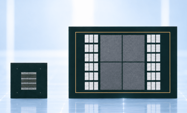
Accordingly, the core competitive factors are considered to be ultra-fine circuit implementation, multi-layerization, and large-area substrate manufacturing technology. The product LG Innotek unveiled is FC-BGA for AI accelerators. It is a large-area substrate with each side exceeding 100 mm. The product incorporates more than 50 years of accumulated substrate-business expertise in ultra-fine circuit and multi-layerization technologies.
At the venue, LG Innotek exhibited a large-area FC-BGA measuring 85 mm by 85 mm. It also displayed an extra-large FC-BGA sample with an area about 40% larger than the 85 mm product. This is part of a strategy to highlight its substrate technology in the trend toward larger high-performance semiconductor packages driven by increasing AI data throughput.
LG Innotek's goal is to mass-produce high-value-added FC-BGA for AI accelerators and for AI training and inference in 2027.
LG Innotek unveiled packaging technology for next-generation FC-BGA. As a representative technology, it introduced Chip Embedding. While conventional methods mount semiconductor chips on the surface of the substrate, the Chip Embedding method inserts the chip inside the substrate. This shortens the connection distance between the chip and the substrate.
A shorter connection distance can improve signal transmission performance and reduce electrical resistance. Lower electrical resistance can also reduce power loss. As AI semiconductors become faster and more highly integrated, the importance of signal integrity and power efficiency inside packages is also increasing. In this regard, Chip Embedding is drawing attention as a next-generation packaging technology.
LG Innotek also introduced glass substrate technology. Glass substrate technology replaces the core-layer material of semiconductor substrates with glass instead of conventional materials. The technology is expected to reduce substrate warping and circuit distortion, making it advantageous for large-area and highly integrated packaging. LG Innotek is developing glass substrate technology and aims to mass-produce glass substrates in 2028.
The exhibition was set up to showcase package substrate products alongside manufacturing technologies, and RF-SiP and FC-CSP were unveiled. LG Innotek displayed the world's No. 1 RF-SiP substrate and also introduced FC-CSP, whose applications are expanding as inference-based AI spreads. Demand for FC-CSP is expanding beyond existing mobile semiconductors to semiconductors for high-performance memory such as GDDR.
On the technology side, the 'Cu-Post' process used in communication semiconductor substrates was introduced as a major exhibit technology. Cu-Post is a method in which fine copper posts are formed on the substrate and solder balls are placed on top to connect the substrate and the main board. Compared with conventional methods, this process can reduce solder-ball spacing to about 20%, allowing more circuits to be placed. The company said Cu-Post can improve substrate heat dissipation by using copper, which has thermal conductivity more than 7 times higher than solder.
LG Innotek showcased display substrates in the tape substrate category, including COF (Chip on Film) and 2-Metal COF. It also presented ECONOVA, a next-generation smart IC substrate, in the tape substrate segment.
ECONOVA is a smart IC substrate that uses a new material capable of delivering high performance without precious-metal plating processes such as palladium (Pd) and gold (Au). Through this, it reduces the use of precious metals while securing both compliance with environmental regulations and product performance.
There is also a trend of expanding demand for eco-friendly materials and manufacturing processes, especially in Europe. Accordingly, demand related to ECONOVA is expected to grow.
At this exhibition, said Jo Ji-tae, head of LG Innotek's Package Solution Division, that the company's substrates can be seen being used across a wide range of industries and everyday applications, including AI, smartphones, and mobility. He also said the company will drive a paradigm shift in the substrate market by putting innovative products at the forefront.
Source: TECHWORLD · Park Gyu-chan
Original: https://www.epnc.co.kr/news/articleView.html?idxno=406707
References
This article was produced with the help of an automated content generation algorithm.
Source: TECHWORLD
View originalThis article was summarized and organized by BizCrush based on the original article from TECHWORLD. For exact quotations and full details, please refer to the original article.