Samsung Electro-Mechanics to Unveil Next-Generation Package Substrates for AI and Servers at KPCA Show 2026
TECHWORLD ·
✦ AI Summary
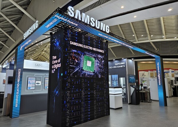
Samsung Electro-Mechanics will participate in 'KPCA Show 2026,' which runs from the 9th to the 11th.
At the exhibition, it will showcase 2.5D and 2.1D package substrates, glass substrates, and next-generation semiconductor package substrate technologies.
Samsung Electro-Mechanics is expanding its application areas to AI and servers, data centers, mobile devices, and automobiles.
As performance improves in AI accelerators and server CPUs, and the use of high-performance memory expands, the importance of package substrates is growing. Semiconductor package substrates connect semiconductor chips to motherboards and handle the transmission of electrical signals and power. As a result, they are emerging as key components that determine semiconductor performance, power efficiency, and signal stability.
Against this backdrop, Samsung Electro-Mechanics plans to unveil next-generation package substrate technologies designed to address the higher performance of semiconductors for AI and servers. Samsung Electro-Mechanics will participate in 'KPCA Show 2026,' which runs from the 9th to the 11th.
KPCA Show is an exhibition for companies related to semiconductor substrates, advanced packaging, materials, and equipment. The event aims to share the industry's latest technologies and market trends.
At this exhibition, Samsung Electro-Mechanics plans to showcase 2.5D and 2.1D package substrates, glass substrates, and next-generation semiconductor package substrate technologies.
AI semiconductors are characterized by the integration of multiple high-performance chips into a single package, and their structural characteristics require advanced package substrate technologies. This calls for large-area, high-layer-count substrate technologies, ultra-fine circuit technologies, fine Via technologies, Bump technologies, and high-precision embedding technologies.
With the expansion of the generative AI market, rising compute performance in AI accelerators, and the rapid increase in data input/output (I/O) volumes, package substrates are increasingly required to deliver large-area, high-layer-count structures, high circuit density, and technologies for implementing a large number of bumps. In response, Samsung Electro-Mechanics presented five exhibition items: 2.5D package substrates, 2.1D package substrates, glass substrates, FCBGA for automotive use, and UTCSP (Ultra Thin Chip Scale Package).
Samsung Electro-Mechanics is expanding the application areas of these exhibition items to AI accelerators and servers, data centers, mobile devices, and automobiles.
Samsung Electro-Mechanics showcased key technologies applied to 2.5D package substrates for AI accelerators. These included large-area, high-layer-count substrate Warpage reduction technology, high-speed signal transmission technology, and high-density interconnection technology. Through these, the company presented a strategy to meet the requirements of high-performance AI semiconductors.
Samsung Electro-Mechanics also unveiled 2.1D package substrate technology. 2.1D packaging does not use a silicon interposer and instead connects semiconductor chips directly through the substrate. Samsung Electro-Mechanics has microcircuit technology and has secured a foundation for high-density interconnection technology. Based on this, it has also secured high-speed, highly integrated chip interconnection technology for AI semiconductors.
AI semiconductors are becoming larger and more highly integrated. Accordingly, interest is increasing in next-generation materials that can address the limitations of conventional organic-material-based package substrates.
Glass substrates are substrates that use glass as the core material. Compared with existing substrates, glass substrates can provide higher rigidity and greater dimensional stability. They can also reduce Warpage in large-area packages and improve signal characteristics and power efficiency. As a result, glass substrates are drawing attention as a next-generation substrate technology for AI semiconductors.
At the exhibition, Samsung Electro-Mechanics will introduce key technologies for realizing glass substrates. These include technology for forming fine interconnect channels in glass materials, metal filling technology for the formed channels, and precision processing technology for glass surfaces. Along with this, the company will also unveil high-value-added package substrate technologies for AI and servers, data centers, mobile devices, and automobiles.
Samsung Electro-Mechanics' UTCSP substrates apply a Coreless structure, which helps reduce substrate thickness. Fine Bond Finger technology is also applied to address the demand for higher integration and slimmer profiles. UTCSP substrate technology targets the package substrate markets for data centers and mobile devices.
The exhibition lineup also includes UTC (Ultra Thin Core) package substrates for CPUs used in laptops and tablets, as well as Co-Package substrates for smartphones. Through these substrates, Samsung Electro-Mechanics will present high-value-added package substrate technologies for multiple applications.
Automotive package substrates require large-area designs, high-layer-count structures, and fine-circuit implementation. They also require high reliability in high-temperature, high-humidity environments and under repeated temperature changes.
Samsung Electro-Mechanics possesses high-function substrate technologies, including multi-chip structures, and plans to strengthen its competitiveness in the automotive package substrate market by emphasizing reliability technologies amid the era of autonomous driving.
Joo Hyuk, head of Samsung Electro-Mechanics' Package Solution Business Division and vice president, said that the high-performance semiconductor market is growing as AI accelerators, servers, and autonomous driving expand, and that the role of package substrates is expanding accordingly while technical difficulty is rising sharply. He added that Samsung Electro-Mechanics plans to enhance large-area, high-layer-count, ultra-fine circuit technologies and next-generation packaging technologies to respond to the high-end semiconductor package substrate market.
Source: TECHWORLD · Park Gyu-chan
Original: https://www.epnc.co.kr/news/articleView.html?idxno=406709
References
This article was produced with the help of an automated content generation algorithm.
Source: TECHWORLD
View originalThis article was summarized and organized by BizCrush based on the original article from TECHWORLD. For exact quotations and full details, please refer to the original article.