Intel Foundry Accelerates High NA EUV Mass Production with ASML, Surpassing 1 Million Wafers
TECHWORLD ·
✦ AI Summary
Intel Foundry and ASML said they are strengthening their collaboration to expand the mass-production adoption of High NA EUV.
The two companies unveiled plans to accelerate industrial adoption of High NA EUV through reticle stitching technology and the buildout of a large-mask ecosystem.
Intel Foundry said it has processed more than 1 million wafers with High NA EUV and has also applied it to some layers of the 18A process and some layers of Panther Lake.
Intel Foundry and ASML are deepening their collaboration to expand the mass-production adoption of High Numerical Aperture (High NA) EUV. High NA EUV is the next-generation extreme ultraviolet (EUV) lithography technology. On the 8th, Intel said the two companies plan to promote industrial adoption of High NA EUV through reticle stitching technology and the buildout of a large-mask ecosystem.
The two companies are pursuing a way to realize the benefits of High NA EUV through reticle stitching technology while using existing 6-inch masks. At the same time, they are also working to build a large-mask ecosystem. The goal is to accelerate industrial adoption of High NA EUV.
Intel Foundry and ASML disclosed the current status of High NA EUV mass-production adoption at the 'SPIE Photomask Technology + Extreme Ultraviolet Lithography' conference held in Monterey, California. They also shared key progress for future technology expansion.
Intel Foundry has processed more than 1 million wafers with High NA EUV to date. Its use spans initial equipment qualification, testing, and research and development (R&D). In addition, it has been applied to mass production of some layers in the code-named 'Panther Lake' Intel Core Ultra Series 3 processor.
Intel said the overlay precision, throughput, and uptime of High NA EUV equipment met initial expectations. That means High NA EUV has moved beyond research and development and reached a stage where it can be used in actual mass-production processes.
Intel said it has applied High NA EUV to some layers of the 18A process. It also said products manufactured using that method performed on par with, or better than, products patterned on the same layers with the ASML NXE platform (NA 0.33 EUV). Intel said the performance advantage, or at least parity, continues to be confirmed.
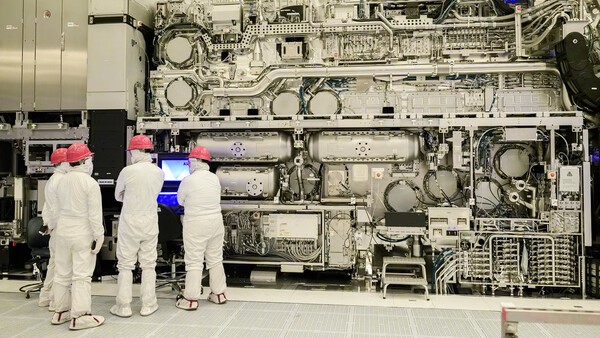
High NA EUV is a technology that uses a higher numerical aperture (NA) than conventional EUV, making it a next-generation lithography technology capable of producing finer patterns. ASML's High NA EUV equipment is the EXE platform, which offers higher resolution than existing EUV tools. The EXE platform is regarded as a key tool for addressing continued pattern shrinking in advanced logic and memory processes.
For High NA EUV to expand broadly across industry, changes are needed not only in lithography equipment but also in the surrounding ecosystem, including masks, pellicles, materials, automation, and EDA. Because High NA EUV requires a different approach to mask usage than conventional EUV, the transition to a large-mask format has been raised as a major issue for the industry.
In this regard, Intel Foundry has made reticle stitching technology that enables the use of existing 6-inch masks a development target. Customers can either plan layer-by-layer layouts based on existing 6-inch masks or use Intel Foundry's stitching capability and process design kit (PDK) solutions.
Reticle stitching is a method in which a single large pattern is exposed in multiple mask regions and then precisely connected. This allows existing mask infrastructure to be used.
The effect of these options is to enable customers to use the benefits of High NA EUV while keeping existing mask specifications in place. As a result, they are expected to ease the burden of transitioning the mask ecosystem when adopting High NA EUV.
Intel Foundry plans to support High NA EUV based on 6-inch masks in the future while also pushing forward a transition to the 6x12-inch large-mask format.
To that end, Intel has led the integration of a mask ecosystem centered on large-mask formats for more than 3 years and has worked with ASML, mask manufacturers, automation suppliers, EDA partners, and materials companies. The scope of collaboration includes standards, infrastructure, and technology development needed to expand High NA EUV.
ASML says it plans to accelerate the expansion of the High NA EUV ecosystem based on its collaboration with Intel Foundry.
Christophe Fouquet, ASML CEO, said Intel Foundry led the introduction of the first commercial EXE system in 2024, validated the adoption of the latest-generation equipment, and achieved the first shipment of a production-type logic product manufactured with High NA. He said Intel Foundry is one of the key leaders driving High NA adoption across the industry.
ASML said Intel Foundry is playing a pioneering role in High NA. It also said it positively views the current value-creation innovations based on 6-inch masks and will provide long-term support for the evolution to 6x12-inch masks.
Naga Chandrasekaran, Intel senior vice president and co-general manager of Intel Foundry, said companies developing increasingly complex AI products need manufacturing innovations that can be applied to mass production immediately and are easy to use. He explained that, from a lithography capability standpoint, Intel Foundry is focusing on short-term support for High NA on 6-inch masks.
Intel Foundry said this focus is unrelated to whether stitching technology is used. It also said it remains focused on the transition to 6x12-inch masks, and Naga Chandrasekaran said he intends to continue working closely with ASML and the broader industry to make that transition a reality.
Intel Foundry and ASML have worked together for years. The two companies are bringing together a large-mask-centered lithography ecosystem and are jointly advancing the standards, infrastructure, and technologies needed for future High NA extreme ultraviolet expansion.
The two companies are working with mask manufacturers, automation suppliers, EDA partners, materials suppliers, and semiconductor manufacturers to build an industry roadmap for the transition to large-mask formats, while also helping customers immediately take advantage of High NA extreme ultraviolet.
Source: TECHWORLD · Park Gyu-chan
Original: https://www.epnc.co.kr/news/articleView.html?idxno=406689
References
This article was produced with the help of an automated content generation algorithm.
Source: TECHWORLD
View originalThis article was summarized and organized by BizCrush based on the original article from TECHWORLD. For exact quotations and full details, please refer to the original article.