Samsung Electronics to Introduce High-NA EUV DRAM in 2028, Expands Next-Gen Chip-Making Cooperation With ASML
TECHWORLD ·
✦ AI Summary
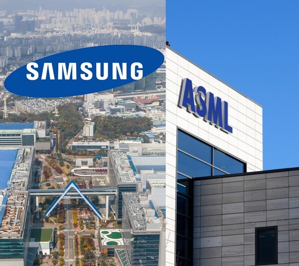
Samsung Electronics announced on the 8th that it will join the 'Large Size Mask Consortium' led by ASML.
Samsung Electronics and ASML will cooperate on joint research for the transition from 6-inch photomasks to 12-inch photomasks and on developing standards related to the 12-inch transition.
Samsung Electronics plans to introduce High-NA EUV lithography equipment into advanced DRAM manufacturing in 2028, and this cooperation is tied to the expansion of High-NA EUV and next-generation 12-inch photomasks.
Samsung Electronics announced on the 8th that it will join the 'Large Size Mask Consortium' led by ASML. ASML is a semiconductor equipment company based in the Netherlands. Through this participation, Samsung Electronics has joined a global consortium developing next-generation 12-inch photomasks, and Samsung Electronics and ASML will expand cooperation in next-generation lithography technology and photomasks.
The two companies plan to carry out joint research collaboration for the transition from 6-inch photomasks to 12-inch photomasks. They will also cooperate on developing standards related to the transition to 12-inch masks.
This cooperation is also aligned with Samsung Electronics' plan to introduce High-NA EUV lithography equipment. Samsung Electronics plans to introduce High-NA EUV lithography equipment into advanced DRAM manufacturing in 2028, with the goal of being the first in the industry to do so.
A photomask is a frame on which semiconductor circuit patterns are precisely etched, and it is a key material that transfers circuit patterns onto wafers using light in the lithography process. As semiconductor miniaturization advances, the impact of photomask precision and lithography technology on semiconductor performance, yield, and productivity is growing even greater.
The mainstream photomask specification in current semiconductor lithography processes is 6 inches. However, as High-NA EUV technology is introduced in earnest, the need for large 12-inch photomasks is expanding.
When using existing 6-inch masks, there are areas where the full pattern cannot be exposed in a single shot, and in such cases a Stitching process is required after dividing the pattern into separate exposures and then connecting them. Samsung Electronics explained that if it switches to 12-inch photomasks, these Stitching constraints will be eased, making it possible to improve advanced semiconductor production efficiency and reduce manufacturing costs.
Advanced semiconductors are characterized by the precise placement of tens of billions of transistors in a very small area, making pattern precision and productivity in the lithography process important. Accordingly, applying 12-inch photomasks is expected to make High-NA EUV equipment performance more effective.
Samsung Electronics has accumulated EUV process experience in memory and foundry. Based on this, Samsung Electronics plans to actively participate in building a large photomask ecosystem.
The cooperation between Samsung Electronics and ASML is not limited to photomasks. Samsung Electronics plans to push ahead with introducing High-NA EUV equipment into advanced DRAM manufacturing by 2028 and to strengthen cooperation for that deployment.
High-NA EUV is a next-generation lithography technology that applies a higher numerical aperture than existing EUV. The NA of existing EUV is 0.33, and the NA of High-NA EUV is 0.55. High-NA EUV makes it possible to implement finer circuit patterns and enables more precise patterning.
As AI data centers spread, demand for high-performance, high-capacity memory is increasing. At the same time, competition to miniaturize DRAM is intensifying.
In this situation, Samsung Electronics plans to extend its DRAM miniaturization roadmap by applying High-NA EUV to advanced DRAM. At the same time, Samsung Electronics plans to pursue process simplification and improve productivity as well.
If High-NA EUV is introduced ahead of others in memory manufacturing, it is expected to make finer circuit implementation possible. It is also expected to improve process efficiency and secure competitiveness in next-generation DRAM.
Samsung Electronics has actively used EUV technology in foundry processes, and it is expanding the scope of next-generation High-NA EUV applications to advanced memory manufacturing as well. This follows Samsung Electronics' strategy to strengthen semiconductor manufacturing competitiveness based on lithography technology.
This move comes amid a surge in demand for AI computing. Accordingly, the importance of high-performance GPU and AI accelerators is growing, and the importance of HBM, advanced DRAM, and more sophisticated foundry processes is also increasing.
In response to these market changes, Samsung Electronics and ASML are expanding cooperation. The significance of this expanded cooperation lies in securing next-generation manufacturing technology to respond to the growth of the AI semiconductor market.
In the semiconductor industry, there is a growing recognition that next-generation lithography technology capable of overcoming miniaturization limits and securing productivity and cost efficiency is a key competitive advantage. Samsung Electronics has maintained a long-term cooperative relationship with ASML.
Samsung Electronics plans to accelerate securing next-generation lithography and manufacturing technologies based on its cooperation with ASML. Through this, Samsung Electronics is expanding the use of EUV and High-NA EUV from foundry to memory.
Executives at Samsung Electronics and ASML explained that the arrival of the AI era is changing the semiconductor industry's paradigm and increasing the importance of technological innovation across the value chain. Samsung Electronics Vice Chairman and CEO Jun Young-hyun said the company plans to continue its leadership in advanced semiconductor manufacturing, including foundry and memory, based on innovative technologies and strong partnerships. He also said Samsung Electronics would strengthen cooperation with ASML and push to establish a technology base for 'Next AI'.
Under this understanding, Samsung Electronics and ASML plan to expand cooperation opportunities in various areas, including advanced memory and next-generation manufacturing methods, based on their existing partnership. ASML CEO Christophe Fouquet said Samsung Electronics has long been one of ASML's key innovation partners, and that the two companies have jointly advanced the foundational technologies of modern semiconductor manufacturing. He said he looks forward to leading next-generation semiconductor manufacturing innovation together with Samsung Electronics in the new era driven by AI. The focus of this cooperation is 12-inch photomasks and High-NA EUV.
This cooperation was viewed as an expansion case in the race to miniaturize semiconductors. It was also presented as an example showing that the competitive landscape is expanding from a focus on 'smaller line widths' to ecosystem competition across lithography equipment, materials, and processes.
Source: TECHWORLD · Park Gyu-chan
Original: https://www.epnc.co.kr/news/articleView.html?idxno=406683
References
This article was produced with the help of an automated content generation algorithm.
Source: TECHWORLD
View originalThis article was summarized and organized by BizCrush based on the original article from TECHWORLD. For exact quotations and full details, please refer to the original article.