Taiwan to Build “Advanced Packaging Hub” in Kaohsiung, Bringing Together Semiconductor Materials and Equipment
TECHWORLD ·
✦ AI Summary
Taiwan is pushing to create a cluster for advanced packaging materials and equipment centered on the Baipu (白埔) Industrial Park in Kaohsiung.
Taiwan's Ministry of Economic Affairs announced the direction for the Baipu Industrial Park on the 1st, and the Ministry of Economic Affairs, SEMI, the Kaohsiung city government and TSMC cooperated.
The Baipu Industrial Park will support R&D, inspection, verification, customer evaluation and deployment to actual production lines, with the goal of drawing together the advanced packaging supply chain and attracting companies to southern Taiwan.
Taiwan is pushing to create a cluster for advanced packaging materials and equipment centered on the Baipu (白埔) Industrial Park in Kaohsiung. The Kaohsiung cluster aims to bring the supply chain for advanced packaging together in southern Taiwan, and the Baipu Industrial Park will be located on a site planned by Kaohsiung City. The park’s development direction is the creation of a materials-and-equipment supply-chain cluster needed for advanced packaging.
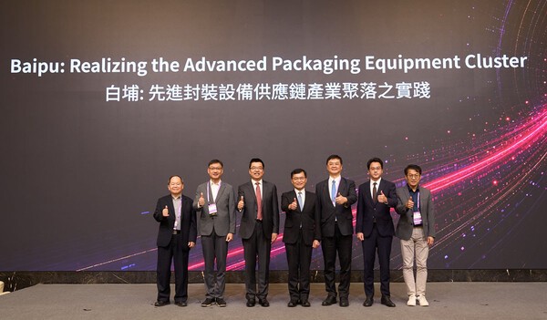
Taiwan's Ministry of Economic Affairs announced the direction for the Baipu (白埔) Industrial Park on the 1st. The announcement was made jointly through cooperation among the Ministry of Economic Affairs, SEMI, the Kaohsiung city government and TSMC. Under a shared infrastructure-building plan, the park will be promoted as a base that brings together companies and related functions for advanced packaging materials and equipment.
The scope of support under the shared infrastructure-building plan covers research and development (R&D), inspection, verification, customer evaluation and deployment to actual production lines. The park's core functions are also focused on supporting major equipment R&D, inspection, verification and on-site manufacturing adoption. In particular, customer evaluation is included as a step that connects materials and equipment that have gone through R&D and inspection and verification to deployment on actual production lines as the advanced packaging supply chain gathers in southern Taiwan.
This cluster will be linked with advanced logic semiconductor and advanced packaging production at the Nanzi Science Industrial Park and Nanzi Science and Technology Industrial Park in Kaohsiung. Through a support system that runs from R&D to verification, customer evaluation and actual production line deployment, Taiwan is seeking to draw the advanced packaging supply chain to southern Taiwan. The strategic goal is to strengthen the semiconductor industrial base in southern Taiwan.
At the Baipu Industrial Park, Taiwan will build a testing and verification platform for advanced packaging equipment and materials by leveraging technologies held by the Industrial Technology Research Institute (ITRI) and the Metal Industries Research & Development Centre (MIRDC), among others.
The platform will be established as a system that supports customer factory-simulation beta site (β-site) evaluation and third-party verification.
Through this, Taiwan plans to promote the commercialization of developed equipment and materials and support their adoption in actual mass-production processes.
At the same time, Taiwan will seek to attract R&D centers of major overseas companies and promote joint development between global conglomerates and Taiwanese small and medium-sized enterprises. Through this, it aims to expand the range of advanced packaging equipment and materials that can be supplied in Taiwan.
This move reflects the backdrop of broader adoption of chiplet and 2.5D and 3D packaging technologies, centered on semiconductors for AI and high-performance computing (HPC). As a result, the need to advance the technological capabilities of advanced packaging equipment and materials is growing.
As semiconductor manufacturing processes become more complex, the need for conditions that allow equipment and materials to be tested and verified close to production sites is increasing. Challenges for semiconductor manufacturing include miniaturization, larger form factors, heterogeneous material bonding and high-precision inspection and metrology, and the importance of an equipment-and-material development and evaluation base in environments close to semiconductor manufacturers is also rising.
In response, Taiwan has set a policy of building a development and verification environment through the Baipu Industrial Park. The goal is to enhance the competitiveness of the advanced packaging ecosystem, while also supporting the entry of existing companies in southern Taiwan into the semiconductor sector.
The procedure for establishing the Baipu Industrial Park is based on Taiwan's Regulations on the Establishment and Management of Science and Technology Industrial Parks. The total area of the park is about 88.73 ha (about 887,300 sq. m), and the planned industrial-only zone covers about 53.63 ha.
Taiwan's Ministry of Economic Affairs plans to hold an information session for companies in the third quarter of 2026. The ministry intends to begin recruiting tenant companies through that session.
Targeted invitees include R&D centers of major overseas companies and semiconductor- and AI-related companies in and outside Taiwan. Taiwan plans to attract companies in connection with the development of the Baipu Industrial Park.
Taiwan has set out a policy of gradually building an industrial cluster centered on advanced packaging materials, manufacturing equipment, inspection and metrology technologies. The cluster will be developed sequentially around capabilities in advanced packaging-related materials, equipment, inspection and metrology.
The Baipu Industrial Park will move forward with efforts to attract new companies. At the same time, it will also support existing manufacturing companies in southern Taiwan as they enter the semiconductor industry.
A Ministry of Economic Affairs official said the ministry will support local companies with processing and manufacturing technologies in shifting their business into semiconductor equipment parts and materials. The official added that the ministry will also support technical cooperation with major semiconductor companies and research institutes, while helping local companies meet semiconductor industry quality standards and technical requirements.
Source: TECHWORLD · Park Kyu-chan
Original: https://www.epnc.co.kr/news/articleView.html?idxno=406523
References
This article was produced with the help of an automated content generation algorithm.
Source: TECHWORLD
View originalThis article was summarized and organized by BizCrush based on the original article from TECHWORLD. For exact quotations and full details, please refer to the original article.