[Tech Report] Benefits of Implementing Self-Driven Synchronous Rectification in an Active-Clamp Forward Converter
TECHWORLD ·
✦ AI Summary
An active-clamp forward converter using self-driven synchronous rectification is described as capable of improving efficiency without a separate isolated secondary-side gate driver.
The article reviews the operating principles and the application limits of conventional self-driven methods, and presents circuit improvements that widen the output-voltage range.
It also introduces verification cases, performance characteristics, and design considerations for an Analog Devices (ADI) active-clamp forward controller.
An active-clamp forward converter with self-driven synchronous rectification is drawing attention because it can improve efficiency without requiring a separate isolated secondary-side gate driver.
This article reviews the operating principles of self-driven synchronous rectification. It then examines the limitations of the approach by explaining the practical constraints of conventional self-driven implementations.
It also explains how the application range can be expanded through simple circuit modifications, extending the approach to both high-output-voltage designs and low-output-voltage designs.
Finally, it presents measurement cases using an active-clamp forward controller to introduce real-world performance and design trade-offs.
Demand for high-current, low-voltage power supplies is rising in communications infrastructure, data centers, industrial automation, and automotive electronics. At the same time, continued increases in load current are making power conversion efficiency, thermal performance, and power density more important.
Against this backdrop, power loss in the output rectification stage has emerged as a key factor that determines overall converter efficiency. As demand rises and load current increases, losses in output rectification have become a critical issue that separates converter performance.
In particular, many isolated DC-DC converter designs identify the secondary-side rectifier diode as a major bottleneck. This bottleneck limits current-handling capability and also constrains achievable thermal performance.
A representative way to reduce such rectification losses is synchronous rectification. This approach replaces the transformer secondary-side rectifier diode with a power MOSFET.
The effect of synchronous rectification is improved power conversion efficiency. That efficiency gain leads to lower power loss and, at the same time, greater thermal headroom.
As a result of reduced power loss and increased thermal headroom, it becomes possible to supply higher continuous output current more reliably. Accordingly, synchronous rectification is presented as a means of improving efficiency and increasing output current.
There are implementation challenges when synchronous rectification is applied to an isolated converter architecture. One example is the need to provide proper gate-drive signals for the secondary-side MOSFET while maintaining isolation from the primary-side controller.
Conventional general-purpose ways to solve this include using a dedicated isolated gate driver. Another conventional approach is to use a complex secondary-side control circuit.
However, conventional methods increase cost. They also bring the drawbacks of greater design complexity and a higher component count.
By contrast, self-driven synchronous rectification can be applied in converter topologies with a limited input-voltage variation range. In general, that input-voltage variation range is within 2x.
Self-driven synchronous rectification is a simple and cost-effective alternative. In this approach, the synchronous rectifier gate-drive signal is obtained directly from the transformer secondary-side voltage, eliminating the need for a separate gate-driver IC.
The benefits become even greater when self-driven operation is combined with an active-clamp forward converter. That is because the waveform generated during reset provides a square-wave form suitable for directly driving the MOSFET gate.
This review focuses on the operating principles of self-driven synchronous rectification for an active-clamp forward converter. Its scope covers an explanation of the basic operating mechanism, an analysis of the main limitations of existing implementations, practical circuit improvements to expand the usable output-voltage range, and verification cases using an Analog Devices (ADI) active-clamp forward controller.
First, the basic operating mechanism of self-driven synchronous rectification for an active-clamp forward converter is explained, followed by an analysis of the main limitations of existing implementations. Next, practical circuit improvements for expanding the usable output-voltage range are presented.
After that, verification cases using an Analog Devices (ADI) active-clamp forward controller are introduced, including performance characteristics and design considerations. This connects the measured performance of the verification cases with the related design considerations.
The active-clamp forward converter is an evolved version of the conventional single-ended forward topology. The design goals of this architecture are improved efficiency and reduced voltage stress on the primary-side switching device.
For background, the transformer reset methods used in conventional forward converters are also presented. Conventional forward converters use either a third reset winding or an RCD clamp circuit.
In this article, the focus is on the operating principles and the limitations of conventional methods centered on self-driven synchronous rectification in the active-clamp forward converter. It then presents a circuit improvement scheme that widens the output-voltage application range, and explains the performance characteristics and design considerations of verification cases based on an Analog Devices (ADI) active-clamp forward controller, while also comparing the reset methods of conventional forward converters with the design goals of the active-clamp structure.
Conventional methods can operate normally. However, they have the disadvantage of dissipating magnetizing energy as heat, and they also impose significant voltage stress on the primary-side switch.
To address these limitations, the active-clamp forward converter uses an active reset circuit. The active reset circuit consists of a clamp capacitor connected in parallel with the transformer primary winding and an auxiliary switch, generally a MOSFET.
During the main switch ON interval, energy from the primary side is transferred to the secondary side, and load power is delivered. At the same time, magnetizing current accumulates in the transformer core.
When the main switch turns OFF, the clamp switch turns ON. During the main switch OFF interval, resonance occurs between the magnetizing current and the clamp capacitor.
The function of this resonance process is to reset the transformer flux. At the same time, the stored energy is recovered without thermal loss, and the recovered energy is reused through the power-transfer path.
This active reset mechanism brings several benefits. Benefit 1 is reduced voltage stress on the primary-side switch, which results from limiting the maximum drain-to-source voltage of the main MOSFET by the clamp capacitor. As a result, low-voltage devices with superior conduction characteristics can be used.
ADI's active-clamp forward controller is described as a way to implement the active-clamp forward converter. The ZVS implementation method in this converter is resonant transition between the main switch and the clamp switch.
This method has the characteristic of enabling ZVS across a wide operating range. The ZVS effect greatly reduces switching losses.
This converter also provides improved EMI performance. The factors behind the EMI improvement are soft switching and controlled voltage transitions, which reduce high-frequency noise generation.
With lower switching losses as the basis, a higher maximum switching frequency also becomes possible. Higher-frequency operation improves power density.
The active-clamp forward converter is a balanced alternative between the simple flyback converter and more complex resonant topologies. This makes it well suited to the excellent efficiency, reliability, and thermal management required in medium- to high-power isolated power systems.
Accordingly, the active-clamp forward converter has broad applicability in medium- to high-power isolated power systems. ADI's active-clamp forward controller is cited as a solution aimed at such uses.
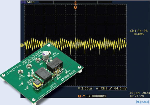
LT3752/LT3752-1 and LT3753 are highly integrated, high-performance active-clamp forward controllers designed to minimize the number of external components. As a result, they can reduce solution size and cost, and all three devices support a single-IC-based power solution.
These products support output power levels up to 400W and offer compact, versatile, high-efficiency power-supply characteristics. This makes it possible to implement a single-IC-based power solution up to 400W.
When higher output is required, power can be scaled by connecting multiple converter outputs in series. The purpose of the series connection is power expansion.
LT3752 and LT3752-1 integrate a fixed-frequency flyback controller that generates housekeeping power for both the primary-side IC and the secondary-side IC, enabling efficient bias-power delivery. This eliminates the need to generate bias power using an auxiliary winding on the main forward transformer, simplifying the transformer structure, reducing transformer size, and lowering cost.
Housekeeping power is used to overdrive the INTVCC pin. This enables external power supply to the IC, improves efficiency, and provides additional gate-drive current. It also serves to keep the INTVCC voltage at an optimal level.
LT3752 is designed to support input voltages up to 100V. It is suitable for communication intermediate bus converters and industrial power supplies.
LT3752-1 extends the operating input-voltage range above 100V. Its main targets are high-voltage automotive battery systems and offline isolated power supplies. LT3753 serves as an additional solution for low-voltage, high-current designs.
These controllers share functions that simplify active-clamp forward design. Common features include configurable switching frequency, current-mode control for fast transient response, a precise programmable volt-second (V-S) clamp, and various protection functions.
When combined with secondary-side self-driven synchronous rectification, they can realize a high-efficiency isolated power solution with minimal components.
This approach directly uses the voltage generated on the transformer secondary winding to drive the secondary-side MOSFET. The source of the gate-drive signal in self-driven synchronous rectification is the induced voltage of the transformer secondary winding.
The target devices are the secondary-side MOSFET. The induced voltage is inherently synchronized with primary-side switching operation.
As a result, no separate control logic is required. It also naturally determines the turn-on and turn-off timing of the synchronous rectification MOSFET.
The application point is the secondary side of the active-clamp forward converter transformer. Two generated waveforms are FSW and CSW. FSW refers to the voltage waveform during the conduction interval of the main forward switch, and CSW refers to the voltage waveform during the conduction interval of the clamp switch during transformer reset.
These waveforms, which are close to square waves, are well suited to directly driving the MOSFET gate. Because their shape is close to a square wave, they are suitable for direct MOSFET gate drive.
If the gates of the synchronous forward MOSFET and synchronous catch MOSFET are properly connected to these signals, the conduction interval of each MOSFET is confined to the correct portion of the switching cycle. As a result, each device conducts only when needed.
The result is a large reduction in conduction loss while performing the same function as conventional rectifier diodes. In other words, the rectifier-diode role is preserved while losses are reduced.
[Figure 1] shows a 5V, 20A active-clamp forward converter operating over a 36V to 72V input-voltage range. The active reset circuit in this example consists of P-channel MOSFET M2 and reset capacitor C7.
In this converter, the clamp capacitor voltage is automatically adjusted according to the duty cycle, ensuring complete transformer flux reset under all operating conditions. In addition, the reset waveform is close to a square wave, so it can be used directly as the gate-drive signal for the secondary-side MOSFET.
[Figure 2] presents the CSW and FSW waveforms used to drive the synchronous forward rectifier and the synchronous catch rectifier.
This configuration is characterized by the absence of a secondary-side controller and the absence of an isolated gate driver.
As a result, it enables cost reduction, lower design complexity, and high power conversion efficiency, while retaining the advantages of self-driven synchronous rectification.
However, the structural limitation of the conventional implementation lies in its dependence on the transformer secondary-side voltage, and the gate-drive voltage for the secondary-side MOSFET is proportional to the converter output voltage.
Under the high-output-voltage condition in Case 1, above 5V, the induced gate-drive voltage may exceed the MOSFET maximum gate-to-source voltage (VGS) rating. Exceeding the VGS rating can reduce long-term reliability, and in severe cases there is also a risk of immediate device damage. By contrast, under the low-output-voltage condition in Case 2, below 2.5V, the gate-drive voltage may be insufficient to fully turn on the MOSFET, and insufficient turn-on can increase conduction loss and reduce overall power conversion efficiency.
The topic is improving the self-driven approach for high-output-voltage applications.
[Figure 3] shows the limitations of a conventional self-driven design. In the conventional self-driven design, the gate-drive voltage magnitude varies together with the output voltage.
Because of this, some improvement to the basic circuit structure is needed to ensure stable operation over a wider output-voltage range.
In particular, when the converter output voltage exceeds about 5V, limiting the gate-to-source voltage (VGS) of the synchronous rectification MOSFET becomes a key challenge.
The simplest solution is to add a secondary auxiliary winding dedicated to gate drive on the transformer. If the winding ratio of the auxiliary winding is properly designed, it can generate a lower gate-drive voltage from the secondary-side voltage.
This lower gate-drive voltage prevents the MOSFET gate voltage from exceeding the allowable operating range.
The auxiliary winding in [Figure 4] provides the gate-drive voltage for the synchronous forward MOSFET and the synchronous catch MOSFET.
In addition, the diodes connected to the CSW and FSW nodes help ensure that the MOSFET turns off at the proper time.
The voltage generated by the auxiliary winding is lower than the main secondary-side voltage.
For this reason, the diodes remain reverse-biased during normal operation, and reverse-biased diodes do not participate in switching operation.
With this simple circuit change, the self-driven synchronous rectification approach can be extended to higher-output-voltage applications without a large increase in design complexity or cost.
Meanwhile, in low-output-voltage designs, another issue arises. Under conditions where VOUT is about 2.5V or lower, it remains difficult to secure sufficient gate-drive voltage to fully turn on the synchronous rectification MOSFET, even when using a secondary winding with an optimized turns ratio.
The conventional approach has the limitation that it cannot maintain proper bias when the characteristics of the steering diode change. For this reason, it is explained that adding only an auxiliary winding cannot solve the limitation.
As a way to solve this limitation, the improved circuit in [Figure 5] is presented. The improved circuit includes an added small-signal MOSFET and an added inductor.
The role of the small-signal MOSFET and the inductor is to form and amplify the usable gate-drive voltage. Thanks to the added components, the gate-drive voltage magnitude can be effectively decoupled from the output voltage, while still maintaining accurate drive timing based on the waveform generated by the transformer.
The application example is a 0.9V, 15A output converter. The benefit of this approach is that it enables efficient synchronous rectification in ultra-low-voltage, high-current applications where diode losses can become excessive.
The drawback of this approach is increased circuit complexity. However, in a comparative evaluation, it is much simpler and more economical than implementing a fully controlled secondary-side gate-driver circuit.
When applying self-driven synchronous rectification to an actual design, practical factors must be reviewed. The inspection items can be divided into component selection, transformer structure, and timing management.
In component selection, the criteria for choosing the MOSFET are important. The criteria are low RDS(ON), an appropriate VGS rating, and a fast internal body diode. These MOSFET characteristics help minimize reverse-recovery losses during switching transitions.
In transformer design, winding arrangement, leakage inductance, and interwinding coupling must be considered. These factors affect waveform quality and switching timing. In addition, the auxiliary winding must be carefully designed with the proper turns ratio to secure the desired gate-drive voltage.
With respect to dead-time control, the self-driven approach inherently provides proper switching timing. However, parasitic elements can cause delays.
These delays can lead to brief simultaneous conduction, or cross-conduction, of the two MOSFETs, or to body-diode conduction. Such problems can be mitigated through proper PCB layout and component selection.
When designing self-driven synchronous rectification, the possibility of insufficient gate-drive voltage during startup and under light-load conditions must also be considered. Stable operation must be ensured under those conditions as well.
If these conditions are carefully addressed in the design, the high power conversion efficiency of synchronous rectification can be fully realized in the actual product.
Self-driven synchronous rectification directly uses the gate-drive signal generated by the transformer. As a result, no separate secondary-side gate driver is required.
Self-driven synchronous rectification reduces cost and design complexity in the active-clamp forward converter. At the same time, it greatly improves power conversion efficiency and current-supplying capability.
This makes it possible to implement a high-efficiency isolated power supply.
The limitation of conventional self-driven approaches is the restricted range of applicable output voltages. However, the application range can be expanded through simple and effective circuit changes, and the expansion targets include both high-output-voltage and low-output-voltage applications.
The techniques presented above can be combined with ADI active-clamp forward controllers. Applied together, they lead to compact, high-performance power solutions that can address a wide range of power-conversion requirements.
The people who explained this are Randyco Prasetyo and Michael Wu. Both are product applications engineers in Analog Devices' HPP group.
Randyco Prasetyo earned a B.S.E.E. from Satya Wacana Christian University in Indonesia. He then studied power electronics at California Polytechnic State University, San Luis Obispo, in the U.S.
Randyco Prasetyo also joined Linear Technology, now part of Analog Devices, in 2011.
Michael Wu is responsible for developing monolithic buck, boost, and buck-boost topologies. He earned his bachelor's and master's degrees in electrical engineering from California Polytechnic State University, San Luis Obispo.
Source: TECHWORLD · Lee Gwang-jae
Original: https://www.epnc.co.kr/news/articleView.html?idxno=406430
References
This article was produced with the help of an automated content generation algorithm.
Source: TECHWORLD
View originalThis article was summarized and organized by BizCrush based on the original article from TECHWORLD. For exact quotations and full details, please refer to the original article.