Hanwha Semitech to Unveil Next-Gen Hybrid Bonder at SEMICON Taiwan
TECHWORLD ·
✦ AI Summary
Hanwha Semitech announced its participation in SEMICON Taiwan 2026.
At the event, which will be held from September 2 to 4 at Nangang Exhibition Center in Taipei, Taiwan, the company will showcase four core advanced packaging equipment products.
The equipment on display will be the large-area FOPLP equipment SFM5 Square, the 3D TC bonder SFM5 Expert, the 2.5D CoW bonder SFM5 TnR, and the hybrid bonder SHB2 Nano.
Hanwha Semitech said it plans to expand into the global market with next-generation advanced packaging equipment. Its main products are large-area fan-out panel-level packaging (FOPLP) equipment and hybrid bonders.
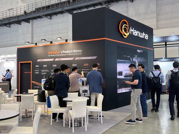
On the 2nd, Hanwha Semitech announced its participation in 'SEMICON Taiwan 2026.' The event will be held from September 2 to 4 at Nangang Exhibition Center in Taipei, Taiwan.
SEMICON Taiwan is an international exhibition where global semiconductor companies gather to share the latest technology and industry trends. This year, more than 1,300 companies from around the world will participate, with Lam Research and Tokyo Electron cited as examples of major exhibitors. Technology cooperation and business partnerships will be discussed at this year's event.
Hanwha Semitech will showcase four core advanced packaging equipment products for high-integration and high-performance semiconductors at booth No. N0984 on the 4th floor of TaiNEX Hall 1.
Four packaging-related equipment products will be introduced together at the exhibition. The four products on display are the large-area FOPLP equipment 'SFM5 Square,' the 3D TC bonder 'SFM5 Expert,' the 2.5D CoW bonder 'SFM5 TnR,' and the hybrid bonder 'SHB2 Nano.' Among them, the actual 'SFM5 Square' large-area FOPLP equipment will be unveiled to customers for the first time.
FOPLP is a technology that uses a 600×600 mm square panel instead of the circular wafer used in conventional semiconductor packaging. The technology offers the advantages of reducing unused area at the edges of the wafer, improving chip placement efficiency, and lowering production costs. 'SFM5 Square' is equipment for precisely mounting semiconductor chips on large panels.
Through this exhibition, Hanwha Semitech plans to present its proprietary technological capabilities for the large-area packaging market to global customers. 'SFM5 Square' is positioned as a means of demonstrating its ability to target the large-area packaging market.
As the importance of the bonding equipment lineup grows amid the expansion of the AI semiconductor and HPC markets, Hanwha Semitech will unveil its related bonding equipment lineup. Among them, the next-generation hybrid bonder 'SHB2 Nano,' developed in February this year, is presented as a key product.
The hybrid bonding used in 'SHB2 Nano' is a direct bonding method for copper electrodes and insulators, differing from conventional bump-and-filler-based methods. This allows chip-to-chip spacing to be minimized, enables thinner and denser semiconductor stacking, and improves data transmission efficiency, drawing attention as a next-generation HBM, advanced memory, and logic packaging technology.
Hanwha Semitech will also exhibit 'SFM5 Expert,' a TC (Thermo-Compression) bonder for HBM production. Hanwha Semitech succeeded in mass production of 'SFM5 Expert' last year, and the equipment is regarded as a key tool for HBM manufacturing. Based on this, the company continues to win orders in related markets and is expanding its technological competitiveness.
Hanwha Semitech introduced 'SFM5 TnR,' an equipment solution for 2.5D packaging. 'SFM5 TnR' is a chip-on-wafer (CoW) bonder that emphasizes its ability to perform precise bonding of semiconductors supplied in different forms on a single machine.
The equipment can process wafer-form logic semiconductors and single HBM units supplied through Tape & Reel. It also features a single-machine processing design for wafer-form logic semiconductors and Tape & Reel-supplied single HBM units.
Hanwha Semitech said this would help reduce intermediate processes and improve productivity. A company official said this year's SEMICON Taiwan is an opportunity to impress the global market with the equipment competitiveness that will lead the era of AI and high-performance packaging, and added that the company will work to expand cooperation with global semiconductor customers and accelerate its entry into the next-generation packaging market.
Hanwha Semitech said it plans to actively promote the technological competitiveness of its advanced packaging equipment to global semiconductor manufacturers at this exhibition. It also said it plans to expand cooperation with customers, strengthen its existing HBM-related equipment business, and broaden its business scope into next-generation packaging markets such as FOPLP.
Source: TECHWORLD · Park Kyu-chan
Original: https://www.epnc.co.kr/news/articleView.html?idxno=406417
References
This article was produced with the help of an automated content generation algorithm.
Source: TECHWORLD
View originalThis article was summarized and organized by BizCrush based on the original article from TECHWORLD. For exact quotations and full details, please refer to the original article.