PIE Unveils Next-Gen Glass Substrate and Advanced Packaging Inspection Solutions at Semicon Taiwan 2026
TECHWORLD ·
✦ AI Summary
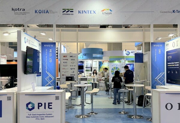
PIE will participate in "Semicon Taiwan 2026," held from the 2nd to the 4th at Taipei Nangang Exhibition Center in Taipei, Taiwan.
At the exhibition, it will unveil its lineup of core inspection equipment for next-generation glass substrates and advanced back-end processes, as well as inspection solutions for Glass Substrate and advanced packaging.
It will showcase the high-resolution TGV AOI, Glass Substrate hole holography inspection system, and X-ray CT and ultrasonic inspection system.
PIE will participate in the semiconductor exhibition "Semicon Taiwan 2026." "Semicon Taiwan 2026" will be held from the 2nd to the 4th at Taipei Nangang Exhibition Center in Taipei, Taiwan. At the show, PIE plans to unveil its lineup of core inspection equipment for next-generation glass substrates and advanced back-end processes, with the exhibition focus set on next-generation inspection solutions for the Glass Substrate process and the high-value-added advanced packaging market. Glass Substrate is emerging as a new game-changer in semiconductor packaging.
Through the exhibition, PIE will introduce its family of inspection equipment targeting Glass Substrate and advanced packaging. Among them, the "high-resolution TGV AOI" is an equipment based on multi-focus inspection technology, designed to perform precision analysis by using the top, middle, and bottom sections of Glass Substrate holes as its inspection range.
PIE also has a "Glass Substrate hole holography inspection system." This equipment applies a refractive index change analysis method to detect material uniformity, and it also includes microcracks and voids among its detection targets.
In addition, PIE also has an "X-ray CT and ultrasonic inspection system." The system is a non-destructive equipment that diagnoses the copper filling status of holes and the ultra-high-stacking status of semiconductor memory.
PIE presented a next-generation inspection lineup for the high-value-added advanced packaging market, including inspection functions for substrate holes used in advanced packaging. The functions unveiled this time include a PTH (Plated Through Hole) inspection function for CCL substrates, a BVH (Blind Via Hole) hole diameter inspection function on ABF (Ajinomoto Build-up Film) and PPG (Prepreg), and a BVH (Blind Via Hole) internal foreign material inspection function on ABF (Ajinomoto Build-up Film) and PPG (Prepreg).
The new next-generation lineup emphasizes the combination of AI vision technology and non-destructive analysis capabilities. With this lineup, PIE aims to expand touchpoints with world-class foundry companies in Taiwan, global OSAT companies, and high-performance substrate manufacturers, while seeking concrete global order opportunities.
Choi Jeong-il, CEO of PIE, said Semicon Taiwan 2026 is an important momentum at a turning point for next-generation materials and advanced packaging transitions. He also said the company will work to strengthen its global recognition for PIE's inspection solutions and deepen local partnerships in Taiwan, while setting a goal of further strengthening its leadership in the global high-precision inspection market for AI semiconductors and advanced packaging.
Source: TECHWORLD · Lee Kwang-jae
Original: https://www.epnc.co.kr/news/articleView.html?idxno=406371
References
This article was produced with the help of an automated content generation algorithm.
Source: TECHWORLD
View originalThis article was summarized and organized by BizCrush based on the original article from TECHWORLD. For exact quotations and full details, please refer to the original article.