Choi Tae-won’s Remarks on Japan Semiconductor Investment Spark Controversy... SK Says It Never Considered Joint Plant
TECHWORLD ·
✦ AI Summary
SK denied reports that Chairman Choi Tae-won was reviewing the establishment of a semiconductor joint plant in Japan.
Choi said in response to a question about Japan investment plans, “We are in the process of studying. As soon as we finish, I'll let you know.”
SK said there were no plans for plant construction, no joint investment plan, and no confirmed review of candidate sites in specific regions.
Some reports claimed that SK Group Chairman Choi Tae-won was considering establishing a semiconductor joint plant in Japan, but SK denied the claim. According to an SK Group statement on the 31st, Choi’s actual remarks were only that the company was currently reviewing investment in Japan more broadly and would let people know when that process was finished.
According to SK’s explanation, Choi’s remarks were limited to, "We are currently reviewing it, and I will let you know when it is finished," and the intended meaning of that response was that it was "currently under review, and we will inform you after the review ends." SK said he did not mention any specific plant construction plan or any plan for a joint investment.
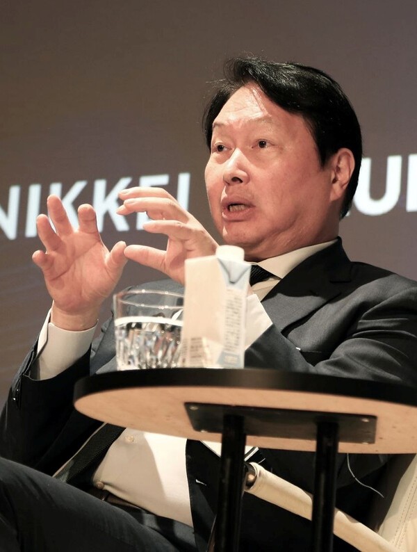
Choi attended a meeting of the Korea-Japan Chamber of Commerce and Industry chairpersons in Sendai, Japan, that day, and when asked about investment plans in Japan, he replied, "We are in the process of studying. As soon as we finish, I'll let you know." However, Choi did not explain whether he would build a semiconductor plant in Japan, and he also did not discuss specific investment methods, candidate sites, or partners.
SK also said it had never considered a joint plant. Accordingly, the company drew a line under reports claiming it was reviewing the establishment of a semiconductor joint plant in Japan, saying they were not true.
Some foreign and domestic media reported that the chairman was reviewing the feasibility of building a joint plant for memory semiconductor production in Japan and was looking at candidate sites across the country. The apparent thrust of the remarks was that any location with abundant power and water would be considered, and candidate sites in places such as Miyagi Prefecture were also mentioned.
In response, SK corrected the facts in the related reports. A SK Group official said Choi’s answer to the question about Japan investment plans was that the matter was at the review stage and that he would let people know as soon as it was finished, explaining that this differed from reports saying Choi had said he was reviewing the establishment of a semiconductor joint plant in Japan.
SK said it could not confirm any review of candidate plant sites in specific regions in Japan at present. It also said there was no confirmed decision on a plant site in regions such as Miyagi Prefecture, and that no such region had been officially designated as a review target.
The only verifiable fact at present is that Choi answered that he was reviewing the possibility of investment in Japan when asked. However, it is difficult to conclude that the answer meant he was pushing ahead with establishing a semiconductor plant in Japan, and it is also difficult to expand that into meaning he was considering a joint plant.
It is pointed out that the cause of the controversy lies more in the way the remarks were amplified during transmission than in Choi’s remarks themselves. Choi’s actual answer did not mention a factory, did not mention a joint venture, and did not mention memory or a site. Based on that, SK denied reports that it was reviewing the establishment of a joint plant.
A similar round of speculation had surfaced in June over Choi’s remarks related to semiconductors in Japan. At the time, Choi said Japan had an ecosystem needed for semiconductor production, including power and materials, and that led to speculation that SK might build a semiconductor plant in Japan. But even then, SK explained that it was not actually reviewing the construction of a semiconductor plant in Japan.
A SK official said SK Hynix is pushing to expand its global production base, citing as evidence the ongoing expansion of domestic semiconductor production facilities and the construction of a cutting-edge packaging base for next-generation HBM production in West Lafayette, Indiana. The official added that expanding the global production network and whether to build a plant in Japan are separate issues.
Source: TECHWORLD · Park Kyu-chan
Original: https://www.epnc.co.kr/news/articleView.html?idxno=406312
References
This article was produced with the help of an automated content generation algorithm.
Source: TECHWORLD
View originalThis article was summarized and organized by BizCrush based on the original article from TECHWORLD. For exact quotations and full details, please refer to the original article.