SK hynix Expands HBM Production System to the U.S., Starts HBM4E Mass Production at Indiana Fab
IT DAILY ·
✦ AI Summary
SK hynix decided to expand HBM production and R&D to the U.S. and establish a dual system between Korea and the U.S.
The company held a groundbreaking ceremony for the 'Indiana Fab' in West Lafayette, Indiana, and the plant is an advanced packaging production base for AI memory that will mass-produce HBM4E.
The company aims to complete the clean room in October 2028 and begin HBM mass production in the second half of 2029, while also pursuing local packaging, testing, and an R&D testbed in the U.S.
As competition in next-generation HBM intensifies, with the importance of custom design and verification aligned to customers' AI computing chip development schedules rising, SK hynix decided to expand production and R&D to the United States, where major customers are based, and broaden its HBM production system to the U.S. Accordingly, it will create a dual production base in Korea and the U.S., build a system in which advanced wafers produced in Korea are packaged and tested in the U.S. before being supplied to local customers, and also set up an R&D testbed in the U.S.
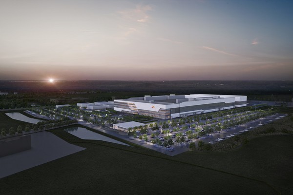
On the 27th local time, SK hynix held a groundbreaking ceremony for the 'Indiana Fab' in West Lafayette, Indiana. The 'Indiana Fab' is an advanced packaging production base for AI memory, with an investment of more than USD 4 billion (about KRW 5.5 trillion). The company plans to complete the clean room in October 2028 and aims to begin mass production of next-generation HBM in the second half of 2029. The 'Indiana Fab' will mass-produce HBM4E.
Kwak Noh-jung, president of SK hynix, said that the product to be manufactured at the Indiana Fab being built in West Lafayette, Indiana, is the 7th-generation HBM, 'HBM4E,' now under development. SK hynix plans to begin mass production of HBM4E at the Indiana Fab in the third quarter of 2029.
The Indiana Fab will house an HBM advanced packaging production line and research and development (R&D) facilities. Once the plant is operational, SK hynix's HBM completion process will run through both Korea and the U.S.
Advanced wafers for HBM will be produced in Korea, shipped to the U.S., then go through advanced packaging and testing before being supplied as finished products to local customers. SK hynix presented this as the first 'Made in USA' HBM produced in the U.S.
This division of labor aligns with changes in HBM technology. HBM is a semiconductor that boosts data processing bandwidth by vertically stacking multiple DRAM chips.
HBM manufacturing requires TSV and precise bonding, and advanced packaging capabilities are critical in the production process. In addition, the importance of coordinating specifications with computing chips such as GPU and application-specific integrated circuits (ASIC) is also growing.
As the base die function of memory after HBM4 becomes more advanced, the importance of customized optimization for each customer's computing system is increasing. Accordingly, collaboration on aligning memory specifications from the early development stage of customers' next-generation AI chips is expanding, along with broader cooperation on prototype verification.
SK hynix's simultaneous establishment of a production line and an advanced packaging R&D testbed within the Indiana Fab is aligned with this trend toward customer-specific collaboration. This initiative will support joint development of next-generation packaging technologies with customers, universities, and partners, and will also back local prototype production and performance verification.
In addition, SK hynix and Purdue University signed a memorandum of understanding (MOU) for joint research on next-generation system integration and advanced packaging technologies, including HBM. The Indiana Fab, the packaging R&D testbed, and the MOU with Purdue University are examples of connecting design coordination and verification collaboration at the early development stage to a local research, production, and verification system.
Building the production base will also expand the supply chain for materials, parts, and equipment. SK hynix said it is discussing expansion into West Lafayette with more than 100 partner companies, and it plans to create about 7,000 direct and indirect jobs with American companies during the construction and operation of the Indiana Fab.
The U.S. government supported the Indiana project through the CHIPS Act. The U.S. Department of Commerce finalized direct grants of up to USD 458 million and loan support of up to USD 500 million for SK hynix. The Commerce Department said the Indiana investment would help strengthen the domestic U.S. supply chain for next-generation HBM and advanced packaging.
At the time the Indiana Fab broke ground, pressure for local semiconductor production in the U.S. was intensifying again. The Trump administration is reportedly reviewing plans to impose high tariffs on semiconductors and some finished goods, and is also considering linking tariff-free volumes to the scale of investment and production in the U.S.
SK hynix's investment in Indiana has been under way since 2024. For that reason, recent tariff discussions are difficult to connect directly to the decision to invest in Indiana. Still, amid pressure for local semiconductor production in the U.S., the strategic value of securing a local HBM back-end processing base is increasing.
Future U.S. trade policy remains a variable. Packaging and testing will take place at the Indiana Fab, but the core wafers will be produced in Korea, so the impact on the Korea-U.S. division of labor could vary depending on how U.S. semiconductor tariff and support policies define the scope of local production.
At the same time, the expansion of HBM is driving changes in how memory companies compete. If the key factor in general-purpose DRAM competition is the productivity and cost competitiveness of standardized products, the key factor in HBM competition is the growing emphasis on specification customization from the customer AI chip development stage.
Accordingly, core capabilities are also changing. Understanding customer product roadmaps and developing and supplying needed products on time are emerging as critical, and the trend of customer collaboration from the product development stage is strengthening.
Greater optimization for each customer is also broadening memory companies' ability to identify demand early. As a result, the timing of demand and supply for next-generation products can be coordinated more proactively than before.
The Indiana Fab shows that customer-centric HBM competition is a case of shifting production base locations. It reflects a trend in which the HBM competitive model is moving toward proximity to customers, influencing where production bases are located.
SK hynix plans to fully activate a local system in the U.S. that connects packaging, verification, and supply for next-generation products in line with the start of HBM4E mass production in 2029, and said it intends to operate this around the Indiana Fab. Kwak said the U.S. is a center of AI innovation where top-tier customers, research capabilities, and ecosystems come together, and explained that the company intends to make the Indiana Fab its first 'Made in USA' HBM supply base.
Source: IT DAILY · Kim Byeong-ju
Original: https://www.itdaily.kr/news/articleView.html?idxno=241282
References
This article was produced with the help of an automated content generation algorithm.
Source: IT DAILY
View originalThis article was summarized and organized by BizCrush based on the original article from IT DAILY. For exact quotations and full details, please refer to the original article.